The structure of the IELTS Academic Writing Task 1 (Report Writing):
Introduction:
Introduction (never copy word for word from the question) + Overview/ General trend (what the diagrams indicate at a first glance).
Reporting Details:
Main features in the Details
+ Comparison and Contrast of the data. (Do not give all the figures.) + Most striking features of the graph.
Conclusion:
Conclusion (General statement + Implications, significant comments) [The conclusion part is optional.]
Tips:
Write the introduction and General trend in the same paragraph. Some students prefer to write the ‘General Trend’ in a separate paragraph and many teachers suggest both to be written in a single paragraph. Unless you have a really good reason to write the general trend in the second paragraph, try to write them both in the first paragraph. However, this is just a suggestion, not a requirement.
Your ‘Introduction (general statement + overall trend/ general trend) should have 75 – 80
words.
DO NOT give numbers, percentages or quantity in your general trend. Rather give the most striking feature of the graph that could be easily understood at a glance. Thus it is suggested to AVOID –
“A glance at the graphs reveals that 70% of the male were employed in 2001 while 40 thousand women in this year had jobs.”
And use a format /comparison like the following:
“A glance at the graphs reveals that more men were employed than their female counterparts in
2001 and almost two-third of females were jobless in the same year. ”
Vocabulary to Start the Report Body:
Just after you finish writing your ‘Introduction’ (i.e. General Statement + General overview/ trend), you are expected to start a new paragraph to describe the main features of the diagrams. This second paragraph is called the ‘Body Paragraph / Report Body”. You can have a single body paragraph/ report body or up to 3, (not more than 3 in any case) depending on the number of graphs provided in the question and the type of these graphs. There are certain phrases you can use to start your body paragraph and the following is a list of such phrases —
As it is presented in the diagram(s)/ graph(s)/ pie chart(s)/ table…
/immutable / level(ed) out/ stabilise/ remain(ed) the same.
No change, a flat,
a plateau.
Examples:
The overall sale of the company increased by 20% at the end of the year.
The expenditure of the office remained constant for the last 6 months but the profit rose by
almost 25%.
There was a 15% drop in the ratio of student enrollment at this University.
The population of the country remained almost the same as it was 2 years ago.
The population of these two cities increase significantly in the last two decades and it is
expected that it will remain stable during the next 5 years.
Tips:
Use ‘improve’ / ‘an improvement’ to describe a situation like economic condition or employment status. To denote numbers use other verbs/nouns like increase.
Do not use the same word/ phrase over and over again. In fact, you should not use a noun or verb form to describe a trend/change more than twice; once is better!
To achieve a high band score you need to use a variety of vocabulary as well as sentence formations. Vocabulary to represent changes in graphs:
The economic inflation of the country increased sharply by 20% in 2008.
There was a sharp drop in industrial production in the year 2009.
The demand for new houses dramatically increased in 2002.
The population of the country dramatically increased in the last decade.
The price of oil moderately increased during the last quarter but as a consequence, the price of daily necessities rapidly went up.
Vocabulary to represent frequent changes in graphs:
Type of Change
Verb form
Noun form
Rapid ups
and downs
wave / fluctuate /
oscillate / vacillate / palpitate
waves / fluctuations /
oscillations / vacillations
/ palpitations
Example:
The price of the goods fluctuated during the first three months of 2017.
The graph shows the oscillations of the price from 1998 to 2002.
The passenger number in this station oscillates throughout the day and in the early morning and evening, it remains busy.
The changes in car production in Japan shows a palpitation for the second quarter of the year.
The number of students in debate clubs fluctuated in different months of the year and rapid ups and downs could be observed in the last three months of this year.
Tips:
DO NOT try to present every single piece of data presented in a graph. Rather pick 5-7 most significant and important trends/ changes and show their comparisons and contrasts.
The question asks you to write a report and summaries the data presented in graphs(s). This is why you need to show the comparisons, contrasts, show the highest and lowest points and the most striking features in your answer, not every piece of data presented in the diagram(s).
Types of Changes/ Differences and Vocabulary to present them:
Vocabulary For Academic IELTS Writing Task 1 (part 1)
Academic IELTS Writing Task 1 question requires you to use several vocabularies to present the data given in a pie/ bar/ line/ mixed graph or to describe a process or a flow chart. Being able to use appropriate vocabularies, presenting the main trend, comparing & contrasting data and presenting thei logical flow of the graph ensure a high band score in your Academic IELTS writing task 1. This vocabulary section aims to help you learn all the vocabularies, phrases and words you need to know and use in your Academic writing task 1 to achieve a higher band score. The examiner will use four criteria to score your response: task achievement, coherence and cohesion, lexical resource, & grammatical range and accuracy. Since “Lexical Resource” will determine 25% of your score in Task 1, you have to enrich your vocabulary to hit a high band score. To demonstrate that you have a great lexical resource, you need to:
Use correct synonyms in your writing.
Use a range of vocabulary.
Do not repeat words and phrases from the exam question unless there is no alternative.
Use some less common vocabulary.
Do not use the same word more than once/twice.
Use precise and accurate words in a sentence.
It is advisable that you learn synonyms and use them accurately in your writing in order to give the impression that you can use a good range of vocabulary.
The general format for writing academic writing task 1 is as follows:
Each part has a specific format and therefore being equipped with the necessary vocabulary will help you answer task 1 efficiently and will save a great deal of time. Vocabulary for the Introduction Part:
Starting
Presentat
ion Type
Verb
Description
The/ the given / the supplied / the presented / the shown / the provided
diagram /
table / figure / illustration / graph / chart / flow chart / picture/ presentation/ pie chart / bar graph/
column graph / line graph / table data/ data / information / pictorial/ process diagram/ map/ pie
the differences… the changes… the number of… information on… data on… the proportion of… the amount of… information on…
data about…
comparative data…
the trend of…
the percentages of…
the ratio of…
how the…
chart and table/ bar graph and pie chart …
figures / gives data on / gives information on/ presents information about/ shows data about/ demonstrates / sketch out/ summarises…
Example :
The diagram shows employment rates among adults in four European countries from 1925
to 1985.
The given pie charts represent the proportion of male and female employees in 6 broad categories, dividing into manual and non-manual occupations in Australia, between 2010 and 2015.
The chart gives information about consumer expenditures on six products in four countries
namely Germany, Italy, Britain and France.
The supplied bar graph compares the number of male and female graduates in three developing countries while the table data presents the overall literacy rate in these countries.
The bar graph and the table data depict the water consumption in different sectors in five
regions.
The bar graph enumerates the money spent on different research projects while the column graph demonstrates the fund sources over a decade, commencing from 1981.
The line graph delineates the proportion of male and female employees in three different sectors in Australia between 2010 and 2015.
Note that, some teachers prefer the “The line graph demonstrates…” instead of “The given line graph demonstrates…”. However, if you write “The given/ provided/ presented….” it would be correct as well.
Tips:
For a single graph use ‘s’ after the verb, like – gives data on, shows/ presents etc. However, if there are multiple graphs, DO NOT use ‘s’ after the verb.
If there are multiple graphs and each one presents a different type of data, you can write which graph presents what type of data and use ‘while’ to show a connection. For example – ‘The given bar graph shows the amount spent on fast food items in 2009 in the UK while the pie chart presents a comparison of people’s ages who spent more on fast food.
Your introduction should be quite impressive as it makes the first impression on the examiner. It either makes or breaks your overall score.
For multiple graphs and/ or table(s), you can write what they present in combination instead of saying which each graph depicts. For example, “The two pie charts and the column graph in combination depicts a picture of the crime in Australia from 2005 to 2015 and the percentages of young offenders during this period.” Caution:
Never copy word for word from the question. If you do, you would be penalised. always paraphrase the introduction in your own words.
General Statement Part:
The General statement is the first sentence (or two) you write in your reporting. It should always deal with:
What + Where + When.
Example: The diagram presents information on the percentages of teachers who have expressed their views about the different problems they face when dealing with children in three Australian schools from 2001 to 2005.
What = the percentages of teachers…
Where = three Australian schools…
When = from 2001 to 2005…
A good General statement should always have these parts.
Vocabulary for the General Trend Part:
In general…
In common…
Generally speaking…
..
It is obvious…
As it is observed…
As a general trend…
As can be seen…
As an overall trend/ As overall trend…
As it is presented…
It can be clearly seen that…
At the first glance…
It is clear,
At the onset…
It is clear that…
A glance at the graph(s) reveals that…
Example:
In general, the employment opportunities increased till 1970 and then declined throughout
the next decade.
As it is observed, the figures for imprisonment in the five mentioned countries show no
overall pattern, rather shows the considerable fluctuations from country to country.
Generally speaking, citizens in the USA had a far better life standard than that of the
remaining countries.
As can be seen, the highest number of passengers used the London Underground station at 8:00 in the morning and at 6:00 in the evening.
Generally speaking, more men were engaged in managerial positions in 1987 than that of
women in New York this year.
As an overall trend, the number of crimes reported increased fairly rapidly until the mid-
seventies, remained constant for five years and finally, dropped to 20 cases a week after 1982.
At a first glance, it is clear that more percentages of native university pupils violated regulations and rules than the foreign students did during this period.
At the onset, it is clear that drinking in public and drink-driving were the most common
reasons for US citizens to be arrested in 2014.
Overall, the leisure hours enjoyed by males, regardless of their employment status, was
Signal processing is a discipline in electrical engineering and in mathematics that deals with analysis and processing of analog and digital signals , and deals with storing , filtering , and other operations on signals. These signals include transmission signals , sound or voice signals , image signals , and other signals etc.
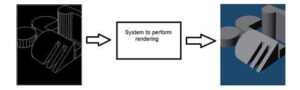
Out of all these signals , the field that deals with the type of signals for which the input is an image and the output is also an image is done in image processing. As it name suggests, it deals with the processing on images.
It can be further divided into analog image processing and digital image processing.
Analog image processing
Analog image processing is done on analog signals. It includes processing on two dimensional analog signals. In this type of processing, the images are manipulated by electrical means by varying the electrical signal. The common example include is the television image.
Digital image processing has dominated over analog image processing with the passage of time due its wider range of applications.
Digital image processing
The digital image processing deals with developing a digital system that performs operations on an digital image.
What is an Image
An image is nothing more than a two dimensional signal. It is defined by the mathematical function f(x,y) where x and y are the two co-ordinates horizontally and vertically.
The value of f(x,y) at any point is gives the pixel value at that point of an image.
The above figure is an example of digital image that you are now viewing on your computer screen. But actually , this image is nothing but a two dimensional array of numbers ranging between 0 and 255.
128 30 123
232 123 321
123 77 89
80 255 255
Each number represents the value of the function f(x,y) at any point. In this case the value 128 ,
230 ,123 each represents an individual pixel value. The dimensions of the picture is actually the dimensions of this two dimensional array.
Relationship between a digital image and a signal
If the image is a two dimensional array then what does it have to do with a signal? In order to understand that , We need to first understand what is a signal?
Signal
In physical world, any quantity measurable through time over space or any higher dimension can be taken as a signal. A signal is a mathematical function, and it conveys some information.
A signal can be one dimensional or two dimensional or higher dimensional signal. One dimensional signal is a signal that is measured over time. The common example is a voice signal.
The two dimensional signals are those that are measured over some other physical quantities.
The example of two dimensional signal is a digital image. We will look in more detail in the
next tutorial of how a one dimensional or two dimensional signals and higher signals are formed and interpreted.
Relationship
Since anything that conveys information or broadcast a message in physical world between two observers is a signal. That includes speech or human voice human voice or an image as a signal. Since when we speak , our voice is converted to a sound wave/signal and transformed with respect to the time to person we are speaking to. Not only this , but the way a digital camera works, as while acquiring an image from a digital camera involves transfer of a signal from one part of the system to the other.
How a digital image is formed
Since capturing an image from a camera is a physical process. The sunlight is used as a source of energy. A sensor array is used for the acquisition of the image. So when the sunlight falls upon the object, then the amount of light reflected by that object is sensed by the sensors, and a continuous voltage signal is generated by the amount of sensed data. In order to create a digital image , we need to convert this data into a digital form. This involves sampling and quantization. The result of sampling and quantization results in an two dimensional array or matrix of numbers which are nothing but a digital image.
Overlapping fields
Machine/Computer vision
Machine vision or computer vision deals with developing a system in which the input is an image and the output is some information. For example: Developing a system that scans human face and opens any kind of lock. This system would look something like this.
Computer graphics
Computer graphics deals with the formation of images from object models, rather then the image is captured by some device. For example: Object rendering. Generating an image from an object model. Such a system would look something like this.
Artificial intelligence
Artificial intelligence is more or less the study of putting human intelligence into machines. Artificial intelligence has many applications in image processing. For example: developing computer aided diagnosis systems that help doctors in interpreting images of X-ray , MRI etc and then highlighting conspicuous section to be examined by the doctor.
Signals
In electrical engineering, the fundamental quantity of representing some information is called a signal. It does not matter what the information is i-e: Analog or digital information. In mathematics, a signal is a function that conveys some information. In fact any quantity measurable through time over space or any higher dimension can be taken as a signal. A signal could be of any dimension and could be of any form.
Analog signals
A signal could be an analog quantity that means it is defined with respect to the time. It is a continuous signal. These signals are defined over continuous independent variables. They are difficult to analyze, as they carry a huge number of values. They are very much accurate due to a large sample of values. In order to store these signals , you require an infinite memory because it can achieve infinite values on a real line. Analog signals are denoted by sin waves.
For example: Human voice
Human voice is an example of analog signals. When you speak, the voice that is produced travel through air in the form of pressure waves and thus belongs to a mathematical function, having independent variables of space and time and a value corresponding to air pressure. Another example is of sin wave which is shown in the figure below. Y = sinx where x is independent
Digital signals
As compared to analog signals, digital signals are very easy to analyze. They are discontinuous signals. They are the appropriation of analog signals.
The word digital stands for discrete values and hence it means that they use specific values to represent any information. In digital signal, only two values are used to represent something i-e: 1 and 0 binary values. Digital signals are less accurate then analog signals because they are the discrete samples of an analog signal taken over some period of time. However digital signals are not subject to noise. So they last long and are easy to interpret. Digital signals are denoted by square waves.
For example: Computer keyboard
Whenever a key is pressed from the keyboard, the appropriate electrical signal is sent to keyboard controller containing the ASCII value that particular key. For example the electrical signal that is generated when keyboard key a is pressed, carry information of digit 97 in the form of 0 and 1, which is the ASCII value of character a.
Difference between analog and digital signals
Comparison element
Analog signal
Digital signal
Analysis
Difficult
Possible to analyze
Representation
Continuous
Discontinuous
Accuracy
More accurate
Less accurate
Storage
Infinite memory
Easily stored
Subject to Noise
Yes
No
Recording Technique
Original signal is preserved
Samples of the signal are taken and preserved
Examples Human voice, Thermometer, Analog phones e.t.c Computers, Digital Phones, Digital pens, etc.
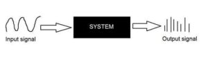
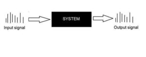
Systems
A system is a defined by the type of input and output it deals with. Since we are dealing with signals, so in our case, our system would be a mathematical model, a piece of code/software, or a physical device, or a black box whose input is a signal and it performs some processing on that signal, and the output is a signal. The input is known as excitation and the output is known as response.
In the above figure a system has been shown whose input and output both are signals but the input is an analog signal. And the output is an digital signal. It means our system is actually a conversion system that converts analog signals to digital signals.
Why do we need to convert an analog signal to digital signal.
The first and obvious reason is that digital image processing deals with digital images, that are digital signals. So when ever the image is captured, it is converted into digital format and then it is processed.
The second and important reason is, that in order to perform operations on an analog signal with a digital computer, you have to store that analog signal in the computer. And in order to store an analog signal, infinite memory is required to store it. And since thats not possible, so thats why we convert that signal into digital format and then store it in digital computer and then performs operations on it.
Continuous systems vs discrete systems Continuous systems
The type of systems whose input and output both are continuous signals or analog signals are called continuous systems.
Discrete systems
The type of systems whose input and output both are discrete signals or digital signals are called digital systems.
Applications of Digital Image Processing
Some of the major fields in which digital image processing is widely used are mentioned below
• Image sharpening and restoration
• Medical field
• Remote sensing
• Transmission and encoding
• Machine/Robot vision
• Color processing
• Pattern recognition
• Video processing
• Microscopic Imaging
Layer 3 network addressing is one of the major tasks of Network Layer. Network Addresses are always logical i.e. these are software based addresses which can be changed by appropriate configurations.
A network address always points to host / node / server or it can represent a whole network. Network address is always configured on network interface card and is generally mapped by system with the MAC address (hardware address or layer-2 address) of the machine for Layer-2 communication.
There are different kinds of network addresses in existence:
IP
IPX
AppleTalk
We are discussing IP here as it is the only one we use in practice these days.
IP addressing provides mechanism to differentiate between hosts and network. Because IP addresses are assigned in hierarchical manner, a host always resides under a specific network.The host which needs to communicate outside its subnet, needs to know destination network address, where the packet/data is to be sent.
Hosts in different subnet need a mechanism to locate each other. This task can be done by DNS. DNS is a server which provides Layer-3 address of remote host mapped with its domain name or FQDN. When a host acquires the Layer-3 Address (IP Address) of the remote host, it forwards all its packet to its gateway. A gateway is a router equipped with all the information which leads to route packets to the destination host.
Routers take help of routing tables, which has the following information:
Method to reach the network
Routers upon receiving a forwarding request, forwards packet to its next hop (adjacent router) towards the destination.
The next router on the path follows the same thing and eventually the data packet reaches its destination.
Network address can be of one of the following:
Unicast (destined to one host)
Multicast (destined to group)
Broadcast (destined to all)
Anycast (destined to nearest one)
A router never forwards broadcast traffic by default. Multicast traffic uses special treatment as it is most a video stream or audio with highest priority. Anycast is just similar to unicast, except that the packets are delivered to the nearest destination when multiple destinations are available.
DC – Network Layer Routing
When a device has multiple paths to reach a destination, it always selects one path by preferring it over others. This selection process is termed as Routing. Routing is done by special network devices called routers or it can be done by means of software processes. The software based routers have limited functionality and limited scope.
A router is always configured with some default route. A default route tells the router where to forward a packet if there is no route found for specific destination. In case there are multiple path existing to reach the same destination, router can make decision based on the following information:
Hop Count
Bandwidth
Metric
Prefix-length Delay
Routes can be statically configured or dynamically learnt. One route can be configured to be preferred over others.
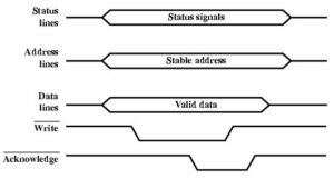
Addressing (Data Communications and Networking)
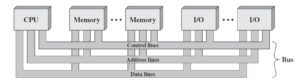
Before you can send a message, you must know the destination address. It is extremely important to understand that each computer has several addresses, each used by a different layer. One address is used by the data link layer, another by the network layer, and still another by the application layer.
When users work with application software, they typically use the application layer address. For example, in next topic, we discussed application software that used Internet addresses (e.g., www.indiana.edu). This is an application layer address (or a server name). When a user types an Internet address into a Web browser, the request is passed to the network layer as part of an application layer packet formatted using the HTTP protocol (Figure 5.6).
The network layer software, in turn, uses a network layer address. The network layer protocol used on the Internet is IP, so this Web address (www.indiana.edu) is translated into an IP address that is 4 bytes long when using IPv4 (e.g., 129.79.127.4) (Figure 5.6). This process is similar to using a phone book to go from someone’s name to his or her phone number.2
The network layer then determines the best route through the network to the final destination. On the basis of this routing, the network layer identifies the data link layer address of the next computer to which the message should be sent. If the data link layer is running Ethernet, then the network layer IP address would be translated into an Ethernet address. Next topic shows that Ethernet addresses are six bytes in length, so a possible address might be 00-0F-00-81-14-00 (Ethernet addresses are usually expressed in hexadecimal) (Figure 1).
Address
Example Software
Example Address
Application layer
Web browser
www.kelley.indiana.edu
Network layer
Internet Protocol
129.79.127.4
Data link layer
Ethernet
00-0C-00-F5-03-5A
Figure 1 Types of addresses
Assigning Addresses
In general, the data link layer address is permanently encoded in each network card, which is why the data link layer address is also commonly called the physical address or the MAC address. This address is part of the hardware (e.g., Ethernet card) and can never be changed.
Network layer addresses are generally assigned by software. Every network layer software package usually has a configuration file that specifies the network layer address for that computer. Network managers can assign any network layer addresses they want.
Application layer addresses (or server names) are also assigned by a software configuration file. Virtually all servers have an application layer address, but most client computers do not. Network layer addresses and application layer addresses go hand in hand, so the same standards group usually assigns both (e.g., https://draftsbook.com/at the application layer means 112.79.78.4 at the network layer). It is possible to have several application layer addresses for the same computer.
Internet Addresses No one is permitted to operate a computer on the Internet unless they use approved addresses. ICANN (Internet Corporation for Assigned Names and Numbers) is responsible for managing the assignment of network layer addresses (i.e., IP addresses) and application layer addresses (e.g https://draftsbook.com/). ICANN sets the rules by which new domain names (e.g., com, .org, .ca, .uk) are created and IP address numbers are assigned to users.
Several application layer addresses and network layer addresses can be assigned at the same time. IP addresses are often assigned in groups, so that one organization receives a set of numerically similar addresses for use on its computers. For example, https://draftsbook.com/has been assigned the set of application layer addresses that end in indiana.edu and iu.edu and the set of IP addresses in the 112.79.x.x range (i.e., all IP addresses that start with the numbers 112.79).
In the old days of the Internet, addresses used to be assigned by class. A class A address was one for which the organization received a fixed first byte and could allocate the remaining three bytes. For example, Hewlett-Packard (HP) was assigned the 15.x.x.x address range which has about 16 million addresses. A class B address has the first two bytes fixed, and the organization can assign the remaining two bytes. https://draftsbook.com/has a class B address, which provides about 65,000 addresses.
People still talk about Internet address classes, but addresses are no longer assigned in this way and most network vendors are no longer using the terminology. The newer terminology is classless addressing in which a slash is used to indicate the address range (it’s also called slash notation). For example 128.192.1.0/24 means the first 24 bits (three bytes) are fixed, and the organization can allocate the last byte (eight bits).
One of the problems with the current address system is that the Internet is quickly running out of addresses. Although the four-byte address of IPv4 provides more than 4 billion possible addresses, the fact that they are assigned in sets significantly limits the number of usable addresses.
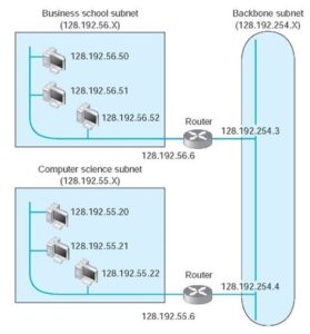
Subnets Each organization must assign the IP addresses it has received to specific computers on its networks. In general, IP addresses are assigned so that all computers on the same LAN have similar addresses. For example, suppose an organization has just received a set of addresses starting with 128.192.x.x. It is customary to assign all the computers in the same LAN numbers that start with the same first three digits, so the business school LAN might be assigned 128.192.56.x, which means all the computers in that LAN would have IP numbers starting with those numbers (e.g., 128.192.56.4, 128.192.56.5, and so on) (Figure 2).
Routers connect two or more subnets so they have a separate address on each subnet. The routers in Figure 2, for example, have two addresses each because they connect two subnets and must have one address in each subnet.
Although it is customary to use the first three bytes of the IP address to indicate different subnets, it is not required. Any portion of the IP address can be designated as a subnet by using a subnet mask.
There are many reasons such as noise, cross-talk etc., which may help data to get corrupted during transmission. The upper layers work on some generalized view of network architecture and are not aware of actual hardware data processing. Hence, the upper layers expect error-free transmission between the systems. Most of the applications would not function expectedly if they receive erroneous data. Applications such as voice and video may not be that affected and with some errors they may still function well.
Data-link layer uses some error control mechanism to ensure that frames (data bit streams) are transmitted with certain level of accuracy. But to understand how errors is controlled, it is essential to know what types of errors may occur.
Types of Errors
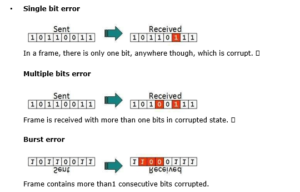
There may be three types of errors:
Single bit error
In a frame, there is only one bit, anywhere though, which is corrupt.
Multiple bits error
Frame is received with more than one bits in corrupted state.
Burst error
Frame contains more than1 consecutive bits corrupted.
Error control mechanism may involve two possible ways:
Error detection
Error correction
Error Detection
Errors in the received frames are detected by means of Parity Check and Cyclic Redundancy Check (CRC). In both cases, few extra bits are sent along with actual data to confirm that bits received at other end are same as they were sent. If the counter-check at receiver’ end fails, the bits are considered corrupted.
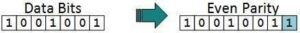
Parity Check
One extra bit is sent along with the original bits to make number of 1s either even in case of even parity, or odd in case of odd parity.
The sender while creating a frame counts the number of 1s in it. For example, if even parity is used and number of 1s is even then one bit with value 0 is added. This way number of 1s remains even.If the number of 1s is odd, to make it even a bit with value 1 is added.
The receiver simply counts the number of 1s in a frame. If the count of 1s is even and even parity is used, the frame is considered to be not-corrupted and is accepted. If the count of 1s is odd and odd parity is used, the frame is still not corrupted.
If a single bit flips in transit, the receiver can detect it by counting the number of 1s. But when more than one bits are erroneous, then it is very hard for the receiver to detect the error.
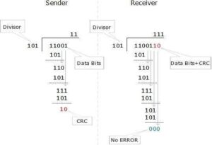
Cyclic Redundancy Check (CRC)
CRC is a different approach to detect if the received frame contains valid data. This technique involves binary division of the data bits being sent. The divisor is generated using polynomials. The sender performs a division operation on the bits being sent and calculates the remainder. Before sending the actual bits, the sender adds the remainder at the end of the actual bits. Actual data bits plus the remainder is called a codeword. The sender transmits data bits as codewords.
At the other end, the receiver performs division operation on codewords using the same CRC divisor. If the remainder contains all zeros the data bits are accepted, otherwise it is considered as there some data corruption occurred in transit.
Error Correction
In the digital world, error correction can be done in two ways:
Backward Error Correction When the receiver detects an error in the data received, it requests back the sender to retransmit the data unit.
Forward Error Correction When the receiver detects some error in the data received, it executes errorcorrecting code, which helps it to auto-recover and to correct some kinds of errors.
The first one, Backward Error Correction, is simple and can only be efficiently used where retransmitting is not expensive. For example, fiber optics. But in case of wireless transmission retransmitting may cost too much. In the latter case, Forward Error Correction is used.
To correct the error in data frame, the receiver must know exactly which bit in the frame is corrupted. To locate the bit in error, redundant bits are used as parity bits for error detection.For example, we take ASCII words (7 bits data), then there could be 8 kind of information we need: first seven bits to tell us which bit is error and one more bit to tell that there is no error.
For m data bits, r redundant bits are used. r bits can provide 2r combinations of information. In m+r bit codeword, there is possibility that the r bits themselves may get corrupted. So the number of r bits used must inform about m+r bit locations plus no-error information, i.e. m+r+1.
2r> = m+r+1
DC – Data-link Control & Protocols
Data-link layer is responsible for implementation of point-to-point flow and error control mechanism.
Flow Control
When a data frame (Layer-2 data) is sent from one host to another over a single medium, it is required that the sender and receiver should work at the same speed. That is, sender sends at a speed on which the receiver can process and accept the data. What if the speed (hardware/software) of the sender or receiver differs? If sender is sending too fast the receiver may be overloaded, (swamped) and data may be lost.
Two types of mechanisms can be deployed to control the flow:
Stop and Wait
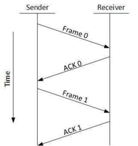
This flow control mechanism forces the sender after transmitting a data frame to stop and wait until the acknowledgement of the data-frame sent is received.
Sliding Window
In this flow control mechanism, both sender and receiver agree on the number of data-frames after which the acknowledgement should be sent. As we learnt, stop and wait flow control mechanism wastes resources, this protocol tries to make use of underlying resources as much as possible.
Error Control
When data-frame is transmitted, there is a probability that data-frame may be lost in the transit or it is received corrupted. In both cases, the receiver does not receive the correct data-frame and sender does not know anything about any loss.In such case, both sender and receiver are equipped with some protocols which helps them to detect transit errors such as loss of data-frame. Hence, either the sender retransmits the data-frame or the receiver may request to resend the previous data-frame.
Requirements for error control mechanism:
Error detection – The sender and receiver, either both or any, must ascertain that there is some error in the transit.
Positive ACK – When the receiver receives a correct frame, it should acknowledge it.
Negative ACK – When the receiver receives a damaged frame or a duplicate frame, it sends a NACK back to the sender and the sender must retransmit the correct frame.
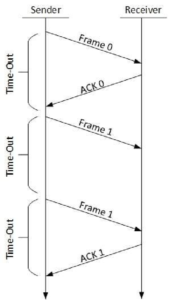
Retransmission: The sender maintains a clock and sets a timeout period. If an acknowledgement of a dataframe previously transmitted does not arrive before the timeout the sender retransmits the frame, thinking that the frame or it’s acknowledgement is lost in transit.
There are three types of techniques available which Data-link layer may deploy to control the errors by Automatic Repeat Requests (ARQ):
Stop-and-wait ARQ
The following transition may occur in Stop-and-Wait ARQ:
The sender maintains a timeout counter.
When a frame is sent, the sender starts the timeout counter. o If acknowledgement of frame comes in time, the sender transmits the next frame in queue. o If acknowledgement does not come in time, the sender assumes that either the frame or its acknowledgement is lost in transit. Sender retransmits the frame and starts the timeout counter.
If a negative acknowledgement is received, the sender retransmits the frame.
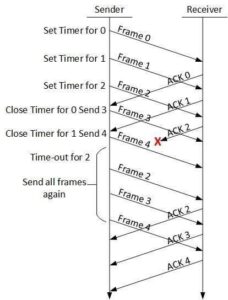
Go-Back-N ARQ
Stop and wait ARQ mechanism does not utilize the resources at their best.When the acknowledgement is received, the sender sits idle and does nothing. In Go-Back-N ARQ method, both sender and receiver maintain a window.
The sending-window size enables the sender to send multiple frames without receiving the acknowledgement of the previous ones. The receiving-window enables the receiver to receive multiple frames and acknowledge them. The receiver keeps track of incoming frame’s sequence number.
When the sender sends all the frames in window, it checks up to what sequence number it has received positive acknowledgement. If all frames are positively acknowledged, the sender sends next set of frames. If sender finds that it has received NACK or has not receive any ACK for a particular frame, it retransmits all the frames after which it does not receive any positive ACK.
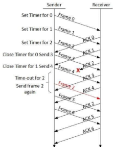
Selective Repeat ARQ
In Go-back-N ARQ, it is assumed that the receiver does not have any buffer space for its window size and has to process each frame as it comes. This enforces the sender to retransmit all the frames which are not acknowledged.
In Selective-Repeat ARQ, the receiver while keeping track of sequence numbers, buffers the frames in memory and sends NACK for only frame which is missing or damaged.
The sender in this case, sends only packet for which NACK is received.
DC – Network Layer Introduction
Layer-3 in the OSI model is called Network layer. Network layer manages options pertaining to host and network addressing, managing sub-networks, and internetworking.
Network layer takes the responsibility for routing packets from source to destination within or outside a subnet. Two different subnet may have different addressing schemes or non-compatible addressing types. Same with protocols, two different subnet may be operating on different protocols which are not compatible with each other. Network layer has the responsibility to route the packets from source to destination, mapping different addressing schemes and protocols.
Layer-3 Functionalities
Devices which work on Network Layer mainly focus on routing. Routing may include various tasks aimed to achieve a single goal. These can be:
Addressing devices and networks.
Populating routing tables or static routes.
Queuing incoming and outgoing data and then forwarding them according to quality of service constraints set for those packets.
Internetworking between two different subnets.
Delivering packets to destination with best efforts.
Provides connection oriented and connection less mechanism.
Network Layer Features
With its standard functionalities, Layer 3 can provide various features as:
Quality of service management
Load balancing and link management
Security
Interrelation of different protocols and subnets with different schema.
Different logical network design over the physical network design.
L3 VPN and tunnels can be used to provide end to end dedicated connectivity.
Internet protocol is widely respected and deployed Network Layer protocol which helps to communicate end to end devices over the internet. It comes in two flavors. IPv4 which has ruled the world for decades but now is running out of address space. IPv6 is created to replace IPv4 and hopefully mitigates limitations of IPv4 too.
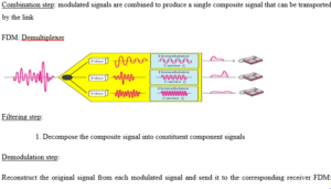
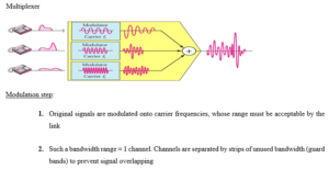
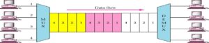
Signal multiplexing is a process in which multiple signals can be transmitted together over the same communication medium simultaneously.
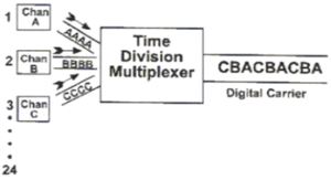
Time division multiplexing
Time division multiplexing is a technique of separating the signals in time domain.
In TDM the transmission from multiple sources take place on the same medium but not at the same time.
The transmissions from various sources are interleaved in time domain. In other words, the data from the various sources is arranged in non contiguous manner by dividing the data into small chunks, which also makes the system efficient.
Pulse code modulation is the most common encoding technique used for TDM digital signals.
PCM system used in North America is a 24-channel system with the sampling rate of 8000 samples per second, 8 bits per sample and a pulse width of 0.625 μs.
We can calculate that sampling interval is 1/8000 = 125 μs, and period required for each pulse group is 8 x 0.625 = 5 μs.
If we transmit only one channel without using the multiplexing technique, then the transmission will contain 8000 frames per second, which will consist of the activity only during the first 5 μs and nothing at all during the rest 120 μs.
Thus will be wasteful and employs complicated method for encoding single channel. Therefore TDM technique is used so that each 125 μs frame is used to provide 24 adjacent channel time slots with the twenty-fifth time slot for synchronization.
Fig1 shows the time division multiplexing of the data from the various channels of the PCM system. TDM finds application in the transmission of SDH and SONET system, GSM telephone system etc.
Fig.1 TDM
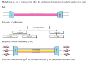
Frequency division multiplexing
Frequency division multiplexing is a technique of separating the signals in frequency domain. In other words, many narrow bandwidth channels are combined and transmitted over a single wide bandwidth transmission system without interfering with each other. Thus FDM takes up a given bandwidth and subdivide it into narrower segments with each segment carrying different information.
FDM is an analog multiplexing scheme where the information entering the FDM system must be analog and it remains analog throughout the transmission.
If the original source information is digital then it must first be converted into equivalent analog signal and then multiplexed in frequency domain.
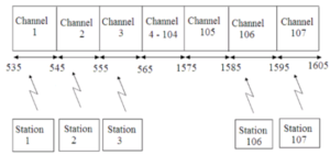
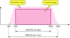
A common example of FDM is the commercial AM broadcast band. 535 kHz to 1605 kHz is the frequency spectrum occupied by the AM band.
Information signal at each broadcast station occupies a bandwidth between 0 Hz and 5 Hz. If we transmit information from each station with the original spectrum, then it would be difficult to differentiate one station’s transmissions from another. Thus to avoid this situation, each station amplitude modulates a different carrier frequency to produce a 10 kHz signal.
Since the carrier frequencies of adjacent stations are separated by 10 kHz signal, the total commercial AM broadcast band is divided into 107 slots with 10 kHz frequency, which are arranged next to each other in the frequency domain.
The receiver tunes in to a particular frequency band associated with the station’s transmission in order to receive that particular station.
The Fig2 shows FDM technique applied to the commercial AM broadcast station for transmission on a common medium.
FDM technique finds application in commercial FM and television broadcasting, telephone and communication systems etc.
Fig.2 FDM
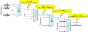
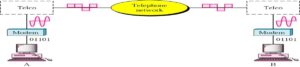
FDM in Telephone Networks
To maximize efficiency, telephone companies have traditionally multiplexed signals from lowerbandwidth lines onto higher-bandwidth lines.
Many switched or leased lines can be combined into fewer but bigger channels
For analog lines, FDM is used
AT&T Analog Hierarchy
Time-Division Multiplexing
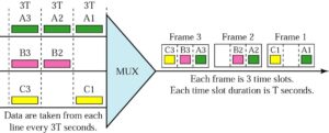
TDM is a digital multiplexing technique to combine data.
TDM: Time Slots and Frames
In a TDM, the data rate of the link is n times faster, and the unit duration is n times shorter.
TDM: Interleaving
Mux: each connection in turn puts a data input into the path
Demux: each connection in turn receives a data unit from the path
TDM: Example 2
4 channels are multiplexed using TDM. If each channel sends 100 bytes/s and we multiplex 1 byte per channel, show the frame traveling on the link, the size of the frame, the duration of a frame, the frame rate, and the bit rate for the link.
TDM: Framing Bits
Mux and Demux may be out of sync => bits are delivered to wrong receivers
Need to separate between frames => extra bits are inserted into the head of each frame. A bit pattern must be followed so that time slots are separated accurately.
T1 Line for Analog Transmission
Analog signal => sampled => TDM
E Lines: Used in Europe
E Line
Rate
Voice
(Mbps)
Channels
E-1
2.048
30
E-2
8.448
120
E-3
34.368
480
E-4
139.26
1920
Multiplexing and Inverse Multiplexing
Input: a data stream
Output: a number of sub-streams each sent over a low-speed line
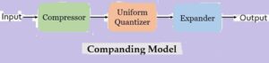
In telecommunication and signal processing companding (occasionally called compansion) is a method of mitigating the detrimental effects of a channel with limited dynamic range. The name is a portmanteau of the words compressing and expanding. The use of companding allows signals with a large dynamic range to be transmitted over facilities that have a smaller dynamic range capability. Companding is employed in telephony and other audio applications such as professional wireless microphones and analog recording.
Model of Companding
The figure below represents the companding model in order to achieve non-uniform companding:
As we can see that the companding model consists of a compressor, a uniform quantizer and an expander.
We have already discussed that companding is formed by merging the compression and expanding. Initially at the transmitting end the signal is compressed and further at the receiving end the compressed signal is expanded in order to have the original signal.
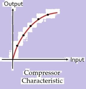
Initially at the transmitting end, the signal is first provided to the compressor. The compressor unit amplifies the low value or weak signal in order to increase the signal level of the applied input signal.
While if the input signal is a high level signal or strong signal then compressor attenuates that signal before providing it to the uniform quantizer present in the model.
This is done in order to have an appropriate signal level as the input to the uniform quantizer. We know a high amplitude signal needs more bandwidth and also is more likely to distort. Similarly, some drawbacks are associated with low amplitude signal and thus there exist need for such a unit.
The operation performed by this block is known as compression thus the unit is called compressor.
The output of the compressor is provided to uniform quantizer where the quantization of the applied signal is performed.
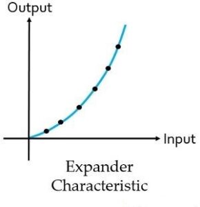
At the receiver end, the output of the uniform quantizer is fed to the expander.
It performs the reverse of the process executed by the compressor. This unit when receives a low value signal then it attenuates it. While if a strong signal is achieved then the expander amplifies it.
This is done in order to achieve the originally transmitted signal at the output.
Characteristic of Compander
As we know companding is composed of compression and expanding. So, here in this session we will separately discuss the compressor and expander characteristic.
Compressor characteristic: The figure below shows the graphical representation of characteristic of the compressor:
The graph clearly represents that the compressor provides high gain to weak signal and low gain to high input signal.
Expander characteristic: Here the figure shows the characteristic of expander:
As we have already discussed that expander performs reverse operation of the compander. So, it is clear from the above figure that artificially boosted signals is attenuated to have the originally transmitted signal.
What is an equalizer?
An equalizer allows the sound in specified frequency bands to be amplified or reduced, in order to adjust the quality and character of the sound. There are different types of equalizer for various uses, such as the parametric equalizers that are controlled using the knobs built into each mixer channel, or the graphic equalizers that allow multiple frequency bands (such as 7, 15, or 31 bands) to be adjusted using sliders.
In general, the most commonly used equalizers are the parametric equalizers equipped on each channel of the mixer. Rarely are the sounds of microphones and instruments that are input to the mixer perfect for delivery as-is to the venue. When mixing music that involves many instruments, some parts may inevitably be difficult to pick out. In this situation, adjusting only volume and panning is not sufficient, and equalizers can be used to adjust each frequency band to make the best characteristics of each instrument stand out.
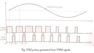
Pulse Position Modulation (PPM)
Definition: A modulation technique that allows variation in the position of the pulses according to the amplitude of the sampled modulating signal is known as Pulse Position Modulation (PPM). It is another type of PTM, where the amplitude and width of the pulses are kept constant and only the position of the pulses is varied.
Simply put, the pulse displacement is directly proportional to the sampled value of the message signal.
Basics of Pulse Position Modulation
The information is transmitted with the varying position of the pulses in pulse position modulation.
The basic idea about the generation of a PPM waveform is that here, as the amplitude of the message signal increases, the pulse shifts according to the reference.
Now, the question arises how the position of the pulses show variation?
A PPM signal is generated in reference to a PWM signal. Thus, the trailing edge of the PWM signal acts as the beginning point of the pulses of PPM signal.
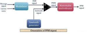
Block diagram for generation of PPM signal
The figure below shows the block diagram for generating a PPM signal:
Here, first, a PAM signal is produced with is further processed at the comparator in order to generate a PWM signal.
The output of the comparator is fed to a monostable multi vibrator. It is negative edge triggered. Hence, with the trailing edge of the PWM signal, the output of the monostable goes high.
This is why a pulse of PPM signal begins with the trailing edge of the PWM signal.
It is to be noted in case of PPM that the duration for which the output will be high depends on the RC components of the multi vibrator. This is the reason why a constant width pulse is obtained in case of the PPM signal.
With the modulating signal, the trailing edge of PWM signal shifts, thus with that shift, the PPM pulses shows shifts in its position.
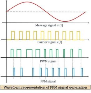
The figure below shows the waveform representation of the PPM signal:
Here, the first image shows the modulating signal, and the second one shows a carrier signal. The next one shows a PWM signal which is considered as reference for the generation of PPM signal shown in the last image.
As we can see in the above figure that the point of ending the PWM pulse and the beginning of PPM pulse is coinciding, which can be clearly seen from the dotted line.
Detection (Demodulation) of PPM signal
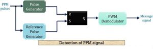
The figure below shows the block diagram for the detection of a PPM signal at the receiver:
The above figure that the demodulation circuit consists of a pulse generator, SR flip-flop, reference pulse generator and a PWM demodulator.
The PPM signal transmitted from the modulation circuit gets distorted by the noise during transmission. This distorted PPM signal reaches the demodulator circuit. The pulse generator employed in the circuit generates a pulsed waveform. This waveform is of fixed duration which is fed to the reset pin (R) of the SR flip-flop.
The reference pulse generator generates, reference pulse of a fixed period when transmitted PPM signal is applied to it. This reference pulse is used to set the flip-flop.
These set and reset signals generate a PWM signal at the output of the flip-flop. This PWM signal is then further processed in order to provide the original message signal.
Advantages of Pulse Position Modulation
Similar to PWM, PPM also shows better noise immunity as compared to PAM. This is so because information content is present in the position of the pulses rather than amplitude.
As the amplitude and width of the pulses remain constant. Thus the transmission power also remains constant and does not show variation.
Recovering a PPM signal from distorted PPM is quite easy.
Interference due to noise in more minimal than PAM and PWM.
Disadvantages of Pulse Position Modulation
In order to have proper detection of the signal at the receiver, transmitter and receiver must be in synchronization.
The bandwidth requirement is large.
Applications of Pulse Position Modulation
The technique is used in an optical communication system, in radio control and in military applications.
Wireless communication takes places over free space through RF (radio frequency), one device, Transmitter send signal to other device, Receiver. Two devices (transmitter and receiver) must use same frequency (or channel) to be able to communicate with each other. If a large number of wireless devices communicate at same time, radio frequency can cause interference with each other. Interference increases as no of devices increases.
Wireless devices share airtime just like wired devices connect to shared media and share common bandwidth. For effective use of media, all wireless devices operate in half duplex mode to avoid collision or interference. Before the transmission begins, devices following IEEE 802.11 standard must check whether channel is available and clear.
Note: Wireless communication is always half duplex as transmission uses same frequency or channel. To achieve full duplex mode, devices uses different frequency or channel of transmission and
receiving of signals. You can say that wireless communication is Full-duplex but technically it is not.
Radio Frequency:
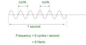
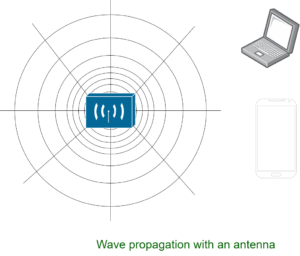
In free space, the sender (transmitter) send an alternating current into a section of wire (an antenna). This sets up a moving electric and magnetic field that away as travelling waves. The electric and magnetic field moves along each other at a right angle to each other as shown. The signal must keep changing or alternating by cycle up and down to keep electric and magnetic field cyclic and pushing forward. The no of cycles a wave taking in a second is called Frequency of the wave.
So,
frequency = no of cycles per second
Electromagnetic waves do not travel in a straight line. they travel by expanding in all direction away from antenna. Like you have seen waves travelling in water when you drop or throw a stone in a water body.
Frequency Unit Names :
Unit
Abbreviation
Meaning
Hertz
Hz
Cycles per second
Kilohertz
KHz
1000 Hz
Megahertz
MHz
1, 000, 000 Hz
Gigahertz
GHz
1, 000, 000, 000 Hz
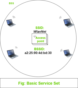
Basic Service Set: We know that wireless communication takes place over the Air. To regulate connection to devices, we need to make every wireless service area a closed group of mobile devices that form around a fixed device. Before mobile devices start data communication, they must advertise their capabilities, and then permission to join should be granted. There is a term defined to such arrangement, IEEE calls this standard a Basic service set (BSS).
At the center of every BSS, there is an access point (AP), it provides services that are necessary to form the infrastructure of Wireless communication. The AP operates in an infrastructure mode and uses a single wireless channel. All devices that want to connect to AP must use that same channel.
Because the operation of BSS depends on AP, BSS is bounded to the area covered by the AP i.e, the area up to which AP’s signal is reachable. This area is called the Basic Service Area (BSA) or cell. The cell is usually a circular shape with the center as AP. The AP serves as a single point of contact for the BSS. The AP uses a unique BSS identifier (BSSID) based on its own MAC address to advertise it’s existence to all devices in the cell.
The AP also advertises a human-readable text string called Service Set identifier (SSID) to uniquely identify the AP. You can say BSSID as a machine-readable unique tag to identify a wireless service and SSID a human-readable service tag.
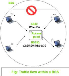
Membership of mobile devices with BSS is called Association. Once associated, the device becomes a BSS client or an 802.11 station (STA). As long as devices are connected to AP, all data communication passes through AP using BSSID as a source and destination address. You can think why all traffic must pass through AP? They can simply communicate with other devices directly without AP as a middleman. If we don’t do so then the whole point of wireless service will go in vain. Sending data through AP make it stable and controllable.
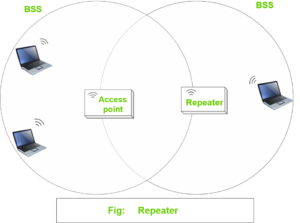
Repeater: An AP in wireless infrastructure usually connected back to the switched networks. BSS has a limited signal coverage area, (BSA). To extend the signal coverage, we can add additional AP but in some scenarios, it is not possible to add additional AP. The solution in such a situation is a Repeater. The repeater is just an AP configured in Repeater mode. A wireless repeater takes a signal as an input and retransmits signals in a new cell around Repeater. The repeater uses two transmitters and receiver to keep the original and repeated signals isolated on a different channel.
Difference between Broadband and Baseband Transmission
S.No
Baseband Transmission
Broadband Transmission
1.
In baseband transmission, the type of signalling used is digital.
In broadband transmission, the type of signalling used is analog.
2.
Baseband Transmission is bidirectional in nature.
Broadband Transmission is unidirectional in nature.
3.
Signals can only travel over short distances.
Signals can be travelled over long distances without being attenuated.
4.
It works well with bus topology.
It is used with a bus as well as tree topology.
5.
In baseband transmission, Manchester and Differential Manchester encoding are used.
Analog-to-analog conversion, or modulation, is the representation of analog information by an analog signal. It is a process by virtue of which a characteristic of carrier wave is varied according to the instantaneous amplitude of the modulating signal. This modulation is generally needed when a bandpass channel is required. Bandpass is a range of frequencies which are transmitted through a bandpass filter which is a filter allowing specific frequencies to pass preventing signals at unwanted frequencies. Representation of analog information by an analog signal
Why do we need it? Analog is already analog!!!
Because we may have to use a band-pass channel
Think about radio…
Analog to Analog Schemes are:
Amplitude modulation (AM)
Frequency modulation (FM)
Phase modulation (PM)
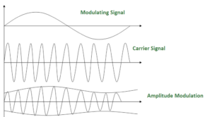
Amplitude Modulation: AM
The modulation in which the amplitude of the carrier wave is varied according to the instantaneous amplitude of the modulating signal keeping phase and frequency as constant.
s(t) = (1+nax(t))cos(2fct)
AM is normally implemented by using a simple multiplier because the amplitude of the carrier signal needs to be changed according to the amplitude of the modulating signal.
AM bandwidth:
The modulation creates a bandwidth that is twice the bandwidth of the modulating signal and covers a range centered on the carrier frequency.
Bandwidth= 2fm
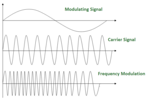
Frequency Modulation: FM
The modulation in which the frequency of the carrier wave is varied according to the instantaneous amplitude of the modulating signal keeping phase and amplitude as constant. The figure below shows the concept of frequency modulation:
FM is normally implemented by using a voltage-controlled oscillator as with FSK. The frequency of the oscillator changes according to the input voltage which is the amplitude of the modulating signal.
FM bandwidth:
The bandwidth of a frequency modulated signal varies with both deviation and modulating frequency.
If modulating frequency (Mf) 0.5, wide band Fm signal.
For a narrow band Fm signal, bandwidth required is twice the maximum frequency of the modulation, however for a wide band Fm signal the required bandwidth can be very much larger, with detectable sidebands spreading out over large amounts of the frequency spectrum.
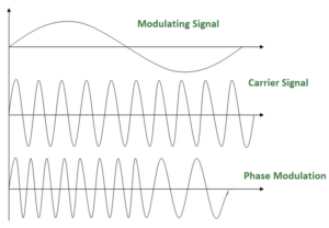
Phase Modulation: PM
Only phase is varied to reflect the change of amplitude in modulating signal
Require simpler hardware than FM
So it can be said, the modulation in which the phase of the carrier wave is varied according to the instantaneous amplitude of the modulating signal keeping amplitude and frequency as constant. The figure below shows the concept of frequency modulation:
Use in some systems as an alternative to FM.
Phase modulation is practically similar to Frequency Modulation, but in Phase modulation frequency of the carrier signal is not increased. It is normally implemented by using a voltage-controlled oscillator along with a derivative. The frequency of the oscillator changes according to the derivative of the input voltage which is the amplitude of the modulating signal.
PM bandwidth:
For small amplitude signals, PM is similar to amplitude modulation (AM) and exhibits its unfortunate doubling of baseband bandwidth and poor efficiency.
For a single large sinusoidal signal, PM is similar to FM, and its bandwidth is approximately, 2 (h+1) Fm where h= modulation index.
Pulse Amplitude Modulation (PAM)
One analog-to-digital conversion method. PAM has some applications, but it is not used by itself in data communication. However, it is the first step in another very popular conversion method called pulse code modulation.
Quantized PAM
Quantization
Method of assigning integral values in a specific range to sampled instance.
Quantizing by using sign and magnitude
Pulse Code Modulation(PCM)
PCM modifies the pulses created by PAM to create a completely digital signal.
Question: What sampling rate is needed for a signal with a bandwidth of 10,000 Hz (1000 to 11,000 Hz)?
The sampling rate must be twice the highest frequency in the signal:
Sampling rate = 2 x (11,000) = 22,000 samples/s
More Question:We want to digitize the human voice. What is the bit rate, assuming 8 bits per sample? The human voice normally contains frequencies from 0 to 4000 Hz.
Sampling rate = 4000 x 2 = 8000 samples/s
Bit rate = sampling rate x number of bits per sample
= 8000 x 8 = 64,000 bps = 64 Kbps
PPM & Delta Modulation
Pulse position modulation (PPM)
In PPM the amplitude and width of the pulses is kept constant but the position of each pulse is varied accordance with the amplitudes of the sampled value of the modulating signal.
The position of the pulses is changed with respect to the position of reference pulses.
The PPM pulses can be derived from the PWM pulses. With the increase in the modulating voltage the PPM pulse shift further with respect to reference.
The vertical dotted lines drawn in Fig are treated as reference lines to measure the shift in position of PPM pulses. The PPM pulses marked 1, 2 and 3 in fig go away from their respective reference lines.
This is corresponding to increase in the modulating signal amplitude. Then as the modulating voltage decreases the PPM pulses 4,5,6,7 come progressively closer to their reference lines.
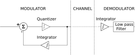
Delta modulation (DM or Δ-modulation) is an analog-to-digital and digital-to-analog signal conversion technique used for transmission of voice information where quality is not of primary importance. DM is the simplest form of differential pulse-code modulation (DPCM) where the difference between successive samples is encoded into n-bit data streams. In delta modulation, the transmitted data is reduced to a 1-bit data stream.
Its main features are:
the analog signal is approximated with a series of segments
each segment of the approximated signal is compared to the original analog wave to determine the increase or decrease in relative amplitude
the decision process for establishing the state of successive bits is determined by this comparison
only the change of information is sent, that is, only an increase or decrease of the signal amplitude from the previous sample is sent whereas a no-change condition causes the modulated signal to remain at the same 0 or 1 state of the previous sample.
To achieve high signal-to-noise ratio, delta modulation must use oversampling techniques, that is, the analog signal is sampled at a rate several times higher than the Nyquist rate.
Derived forms of delta modulation are continuously variable slope delta modulation, delta-sigma modulation, and differential modulation. The Differential Pulse Code Modulation is the super set of DM.
Principle
Rather than quantizing the absolute value of the input analog waveform, delta modulation quantizes the difference between the current and the previous step, as shown in the block diagram in Fig. 1.
Fig. 1 – Block diagram of a Δ-modulator/demodulator
The modulator is made by a quantizer which converts the difference between the input signal and the average of the previous steps. In its simplest form, the quantizer can be realized with a comparator referenced to 0 (two levels quantizer), whose output is 1 or 0 if the input signal is positive or negative. The demodulator is simply an integrator (like the one in the feedback loop) whose output rises or falls with each 1 or 0 received. The integrator itself constitutes a low-pass filter.
For vector computations this kind of processor was designed. A vector is an array of operands of the same type. Consider the following vectors:
Vector A (a1, a2, a3, ……., an)
Vector B (b1, b2, b3,……., bn)
Vector C = Vector A + Vector B
= C(c1, c2, c3, …….,cn), where c1 = a1+ b1, c2 = a2 + b2, …..,Cn= an + bn.
A vector processor adds all the elements of vector A and Vector B using a single vector instruction with hardware approach.
Examples:
DEC’s VAX 9000, IBM 390/VF,CRAY Research Y-MP family, and Hitachi’s S-810/20, etc.
Array Processors or SIMD Processors:
This Array processors are also designed for vector computations. The key difference between an array processor and a vector processor is a vector processor uses multiple vector pipelines, on the other hand an array processor deploys a number of processing elements to operate in parallel. An array processor contains multiple numbers of ALUs. Each ALU is provided with the local memory. The ALU together with the local memory is called a Processing Element (PE). An array processor is a SIMD (Single Instruction Multiple Data) processor. So using a single instruction, the same operation can be performed on an array of data which makes it suitable for vector computations.
Types of Microprocessors
Scalar and Superscalar Processors:
A processor executes scalar data is called scalar processor. The simplest scalar processor makes processing of only integer instruction using fixed-points operands. A powerful scalar processor makes processing of both integer as well floating- point numbers. It contains an integer ALU and a Floating Point Unit (FPU) on the same CPU chip.
A scalar processor may be RISC processor or CISC processor.
Examples of CISC processors are: Intel 386, 486; Motorola’s 68030, 68040; etc. Examples of RISC scalar processors are: Intel i860, Motorola MC8810, SUN’s SPARC CY7C601, etc.
A superscalar processor has multiple pipelines and executes more than one instruction per clock cycle. Examples of superscalar processors are: Pentium, Pentium Pro, Pentium II, Pentium III, etc.
Other Three Types of Microprocessors namely, CISC, RISC, and EPIC.
They are as follows:
1. CISC (Complex Instruction Set Computer)
As the name suggests, the instructions are in a complex form. It means that a single instruction can contain many low-level instructions. For example loading data from memory, storing data to the memory, performing basic operations, etc. Besides, we can say that a single instruction has multiple addressing modes. Furthermore, as there are many operations in single instruction they use very few registers.
Examples of CISC are: Intel 386, Intel 486, Pentium, Pentium Pro, Pentium II, etc.
2. RISC (Reduced Instruction Set Computer)
As per the name, in this, the instructions are quite simple, and hence, they execute quickly. Moreover, the instructions get complete in one clock cycle and also use a few addressing modes only. Besides, it makes use of multiple registers so that interaction with memory is less.
Examples are IBM RS6000, DEC Alpha 21064, DEC Alpha 21164, etc.
It allows the instructions to compute parallelly by making use of compilers. Moreover, the complex instructions also process in fewer clock frequencies. Furthermore, it encodes the instructions in 128-bit bundles. Where each bundle contains three instructions encoded in 41 bits each and a 5-bit template. This 5-bit template contains information about the type of instructions and that which instructions can be executed in parallel.
Digital Signal Processors (DSP):
DSP microprocessors specifically designed to process signals. They receive some digitized signal information, perform some mathematical operations on the information and give the result to an output device. They implement integration, differentiation, complex fast Fourier transform, etc. using hardware.
Examples of digital signal processors are:
Texas instruments’ TMS 320C25, Motorola 56000, National LM 32900, Fujitsu MBB 8764, etc.
Symbolic Processors
Symbolic processors are designed for expert system, machine intelligence, knowledge based system, pattern-recognition, text retrieval, etc. The basic operations which are performed for artificial intelligence are: Logic interference, compare, search, pattern matching, filtering, unification, retrieval, reasoning, etc. This type of processing does not require floating point operations. Symbolic processors are also called LISP processors or PROLOG processors.
Bit-Slice Processors:
The processor of desired word length is developed using the building blocks. The basic building block is called Bit-Slice where the building blocks include 4-bit ALUs, micro programs sequencers, carry look-ahead generators, etc. The word ‘slice’ was used because the desired number of ALUs and other components were used to build an 8-bit, 16-bit or 32-bit CPU.
In a multiprocessor system, a transputer is a specially designed microprocessor to operate as a component processor. Transputers were introduced in late 1980’s. They were built on VLSI chip and contained a processor, memory and communication links. The communication link was to provide point-to-point connection between transputers. A transputer contains FPU, on-chip RAM, high-speed serial link, etc.
Examples of transputers are: INMOS T414, INMOS T800, etc. Where, T414 was a 32-bit processor with 2 KB memory. The T800 was FPU version of 32-bit transputer with 4 KB memory.
Graphic Processors
Graphics Processors are specially designed processors for graphics. Intel has developed Intel 740-3D graphics chip. It is optimized for Pentium II PCs, using a hyper pipelined 3D architecture with additional 2D acceleration. Like most 3D graphics chips, the I-740 will be marketed in performance, not the main stream category. It is designed mostly for such heavy multimedia uses as games and movies.
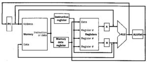
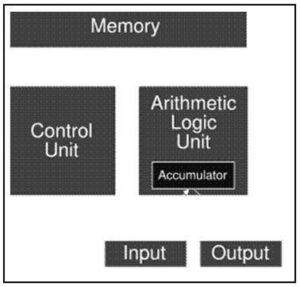
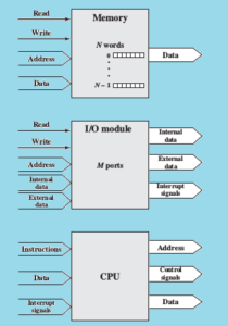
A processor is an integrated electronic circuit that performs the calculations that run a computer. A processor performs arithmetical, logical, input/output (I/O) and other basic instructions that are passed from an operating system (OS). Most other processes are dependent on the operations of a processor.
The terms processor, central processing unit (CPU) and microprocessor are commonly linked as synonyms. Most people use the word “processor” interchangeably with the term “CPU” nowadays, it is technically not correct since the CPU is just one of the processors inside a personal computer (PC).
The Graphics Processing Unit (GPU) is another processor, and even some hard drives are technically capable of performing some processing.
Details of Processor
Processors are found in many modern electronic devices, including PCs, smartphones, tablets, and other handheld devices. Their purpose is to receive input in the form of program instructions and execute trillions of calculations to provide the output that the user will interface with.
A processor includes an arithmetical logic and control unit (CU), which measures capability in terms of the following:
Ability to process instructions at a given time.
Maximum number of bits/instructions.
Relative clock speed.
Every time that an operation is performed on a computer, such as when a file is changed or an application is open, the processor must interpret the operating system or software’s instructions. Depending on its capabilities, the processing operations can be quicker or slower, and have a big impact on what is called the “processing speed” of the CPU.
Each processor is constituted of one or more individual processing units called “cores”. Each core processes instructions from a single computing task at a certain speed, defined as “clock speed” and measured in gigahertz (GHz). Since increasing clock speed beyond a certain point became technically too difficult, modern computers now have several processor cores (dual-core, quad-core, etc.). They work together to process instructions and complete multiple tasks at the same time.
Modern desktop and laptop computers now have a separate processor to handle graphic rendering and send output to the display monitor device. Since this processor, the GPU, is specifically designed for this task, computers can handle all applications that are especially graphic-intensive such as video games more efficiently.
A processor is made of four basic elements: the arithmetic logic unit (ALU), the floating point unit (FPU), registers, and the cache memories. The ALU and FPU carry basic and advanced arithmetic and logic operations on numbers, and then results are sent to the registers, which also store instructions. Caches are small and fast memories that store copies of data for frequent use, and act similarly to a random access memory (RAM).
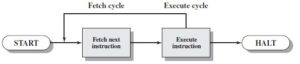
The CPU carries out his operations through the three main steps of the instruction cycle: fetch, decode, and execute.
Fetch: the CPU retrieves instructions, usually from a RAM.
Decode: a decoder converts the instruction into signals to the other components of the computer.
Execute: the now decoded instructions are sent to each component so that the desired operation can be performed.
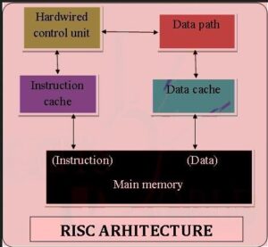
Reduced Set Instruction Set Architecture (RISC)
The main idea behind is to make hardware simpler by using an instruction set composed of a few basic steps for loading, evaluating and storing operations just like a load command will load data, store command will store the data.
Instruction take single clock cycle to get executed.
More number of general purpose register.
Simple Addressing Modes.
Less Data types.
Pipeling can be achieved.
Complex Instruction Set Architecture (CISC)
The main idea is to make hardware complex as a single instruction will do all loading, evaluating and storing operations just like a multiplication command will do stuff like loading data, evaluating and storing it.
Instruction may take more than single clock cycle to get executed.
Less number of general purpose register as operation get performed in memory itself.
Complex Addressing Modes.
More Data types.
Both approaches try to increase the CPU performance.
RISC: Reduce the cycles per instruction at the cost of the number of instructions per program.
CISC: The CISC approach attempts to minimize the number of instructions per program but at the cost of increase in number of cycles per instruction.
Earlier when programming was done using assembly language, a need was felt to make instruction do more task because programming in assembly was tedious and error prone due to which CISC architecture evolved but with uprise of high level language dependency on assembly reduced RISC architecture prevailed.
Example – Suppose we have to add two 8-bit number:
CISC approach: There will be a single command or instruction for this like ADD which will perform the task.
RISC approach: Here programmer will write first load command to load data in registers then it will use suitable operator and then it will store result in desired location.
So, add operation is divided into parts i.e. load, operate, store due to which RISC programs are longer and require more memory to get stored but require less transistors due to less complex command.
Difference Between RISC and CISC
RISC
CISC
Focus on software
Focus on hardware
Transistors are used for more registers
Transistors are used for storing complex
Instructions
Code size is large
Code size is small
A instruction execute in single clock cycle
Instruction take more than one clock cycle
A instruction fit in one word
Instruction are larger than size of one word
RISC uses transistors for more registers.
Transistors are used for storing the complex instructions.
The instructions have a fixed size.
The size of instructions vary.
It performs only register to register arithmetic operations.
Besides the register to register operations, it can also perform register to memory (or memory to register operations).
Fewer registers are used.
It requires more number of registers.
As the instructions are individual the code is large.
Multiple operations are present in single instruction hence, the code is small.
As with the single-cycle and multi-cycle implementations, we will start by looking at the datapath for pipelining. We already know that pipelining involves breaking up instructions into five stages:
IF – Instruction Fetch
ID – Instruction Decode
EX – Execution
MEM – Memory Access WB – Write Back
We will start by taking a look at the single-cycle datapath, divided into stages bu following figure
Figure 1
The Pipeline Registers
IF/ID This provides an execution context for the ID (Instruction Decode and Register Fetch) stage of execution.
ID/EX This provides an execution context for the EX (Execute) phase of instruction execution. In particular, the discrete control signals generated by the control unit as a result of instruction decoding are stored here.
EX/MEM This provides an execution context for the MEM (Memory Access or R-Type Instruction Completion) phase of instruction execution. In addition , this register stores copies of the control signals required to complete both the MEM and WB phase of execution for this instruction.
MEM/WB This provides an execution context for the WB (Write Back) phase of instruction execution.
As we can see, each of the steps maps nicely in order onto the single-cycle datapath. Instruction fields and data generally move from left-to-right as they progress through each stage. The two exceptions are:
The WB stage places the result back into the register file in the middle of the datapath à leads to data hazards.
The selection of the next value of the PC – either the incremented PC or the branch address à leads to control hazards.
One way to visualize pipelining is to consider the execution of each instruction independently, as if it has the datapath all to itself. We can place these datapaths on a timeline to see their relationship. The stages are represented by the datapath element being used, shaded according to use.
Figure 2
In reality, these instructions are not executing in their own datapaths, they share a datapath.
The first instruction uses instruction memory in its IF stage in cycle 1. Then, in cycle 2, the second instruction uses instruction memory for its own IF stage.
Datapath Partitioning for Pipelining
Recall Figure 2 the single-cycle datapath, which can be partitioned (subdivided) into functional units as shown in Figure 2. Because the single-cycle datapath contains separate Instruction Memory and Data Memory units, this allows us to directly implement in hardware the IF-ID-EX-MEM-WB representation of the MIPS instruction sequence. Observe that several control lines have been added, for example, to route data from the ALU output (or memory output) to the register file for writing. Also, there are again three ALUs, one for ALUop, another for JTA computation, and a third for adding PC+4 to compute the address of the next instruction.
Partitioning of the MIPS single-cycle datapath developed previously, to form a pipeline processor. The segments are arranged horizontally, and data flows from left to right.
We can represent this pipeline structure using a space-time diagram similar . Here four load instructions are executed sequentially, which are chosen because the lw instruction is the only one in our MIPS subset that consistently utilizes all five pipeline segments. Observe also that the right half of the register file is shaded to represent a read operation, while the left half is shaded to represent write.
Partitioning of the MIPS single-cycle datapath developed previously, with replication in space, to form a pipeline processor that computes four lw instructions. The segments are arranged horizontally, and data flows from left to right, synchronously with the clock cycles (CC1 through CC7).
In order to ensure that the single-cycle datapath conforms to the pipeline design constraint of one cycle per segment, we need to add buffers and control between stages, similar to the way we added buffers in the multicycle datapath. These buffers and control circuitry are shown in Figure 5.4 as red rectangles, and store the results of the i-th stage so that the (i+1)-th stage can use these results in the next clock cycle.
In summary, pipelining improves efficiency by first regularizing the instruction format, for simplicity. We then divide the instructions into a fixed number of steps, and implement each step as a pipeline segment. During the pipeline design phase, we ensure that each segment takes about the same amount of time to execute as other segments in the pipeline. Also, we want to keep the pipeline full wherever possible, in order to maximize utilization and throughput, while minimizing set-up time.
For this to work, we need to add registers to store data between cycles.
This figure shows the addition of pipeline registers (in blue) which are used to hold data between cycles.
Following our laundry analogy, these might be like baskets between the washer, dryer, etc that hold a clothing load between steps. During each cycle, an instruction advances from one pipeline register to the next pipeline register. Note that the registers are labeled by the stages that they separate.
Pipeline registers are as wide as necessary to hold all of the data passed into them. For instance, IF/ID is 64 bits wide because it must hold a 32-bit instruction and a 32-bit PC+4 result.
Pipelined data path and control
A pipeline processor can be represented in two dimensions, as shown in Figure 1. Here, the pipeline segments (Seg #1 through Seg #3) are arranged vertically, so the data can flow from the input at the top left downward to the output of the pipeline (after Segment 3). The progress of an instruction is charted in blue typeface, and the next instruction is shown in red typeface.
There are three things that one must observe about the pipeline
First, the work (in a computer, the ISA) is divided up into pieces that more or less fit into the segments alloted for them.
Second, this implies that in order for the pipeline to work efficiently and smoothly, the work partitions must each take about the same time to complete. Otherwise, the longest partition requiring time T would hold up the pipeline, and every segment would have to take time T to complete its work. For fast segments, this would mean much idle time.
Third, in order for the pipeline to work smoothly, there must be few (if any) exceptions or hazards that cause errors or delays within the pipeline. Otherwise, the instruction will have to be reloaded and the pipeline restarted with the same instruction that causes the exception. There are additional problems we need to discuss about pipeline processors, which we will consider shortly.
It is easily verified, through inspection of Figure 1., that the response time for any instruction that takes three segments must be three times the response time for any segment, provided that the pipeline was full when the instruction was loaded into the pipeline. As we shall see later in this section, if an N-segment pipeline is empty before an instruction starts, then N + (N-1) cycles or segments of the pipeline are required to execute the instruction, because it takes N cycles to fill the pipe.
Work Partitioning. In the previous section, we designed a multicycle datapath based on the assumption that computational work associated with the execution of an instruction could be partitioned into a five-step process, as follows:
Performance. Because there are N segments active in the pipeline at any one time (when it is full), it is thus possible to execute N segments concurrently in any cycle of the pipeline. In contrast, a purely sequential implementation of the fetch-decode-execute cycle would require N cycles for the longest instruction. Thus, it can be said that we have O(N) speedup. As we shall see when we analyze pipeline performance, an exact N-fold speedup does not always occur in practice. However it is sufficient to say that the speedup is of order N.
Pipeline Datapath Design and Implementation
The work involved in an instruction can be partitioned into steps labelled IF (Instruction Fetch), ID (Instruction Decode and data fetch), EX (ALU operations or R-format execution), MEM (Memory operations), and WB (Write-Back to register file). We next discuss how this sequence of steps can be implemented in terms of MIPS instructions.
MIPS Instructions and Pipelining
In order to implement MIPS instructions effectively on a pipeline processor, we must ensure that the instructions are the same length (simplicity favors regularity) for easy IF and ID, similar to the multicycle datapath. We also need to have few but consistent instruction formats, to avoid deciphering variable formats during IF and ID, which would prohibitively increase pipeline segment complexity for those tasks. Thus, the register indices should be in the same place in each instruction. In practice, this means that the rd, rs, and rt fields of the MIPS instruction must not change location across all MIPS pipeline instructions.
Additionally, we want to have instruction decoding and reading of the register contents occur at the same time, which is supported by the datapath architecture that we have designed thus far. Observe that we have memory address computation in the lw and sw instructions only, and that these are the only instructions in our five-instruction MIPS subset that perform memory operations. As before, we assume that operands are aligned in memory, for straightforward access.
In the next section, we will see that pipeline processing has some difficult problems, which are called hazards, and the pipeline is also susceptible to exceptions.
Pipeline Control and Hazards
The control of pipeline processors has similar issues to the control of multicycle datapaths. Pipelining leaves the meaning of the nine control lines unchanged, that is, those lines which controlled the multicycle datapath. In pipelining, we set control lines (to defined values) in each stage for each instruction. This is done in hardware by extending pipeline registers to include control information and circuitry.
Pipeline Control Issues and Hardware
Observe that there is nothing to control during instruction fetch and decode (IF and ID). Thus, we can begin our control activities (initialization of control signals) during ID, since control will only be exerted during EX, MEM, and WB stages of the pipeline. Recalling that the various stages of control and buffer circuitry between the pipeline stages are labelled IF/ID, ID/EX, EX/MEM, and MEM/WB, we have the propagation of control shown in Figure.
Propagation of control through the EX, MEM, and WB states of the MIPS pipelined datapath.
Here, the following stages perform work as specified:
IF/ID: Initializes control by passing the rs, rd, and rt fields of the instruction, together with the opcode and funct fields, to the control circuitry.
ID/EX: Buffers control for the EX, MEM, and WB stages, while executing control for the EX stage. Control decides what operands will be input to the ALU, what ALU operation will be performed, and whether or not a branch is to be taken based on the ALU Zero output.
EX/MEM: Buffers control for the MEM and WB stages, while executing control for the MEM stage. The control lines are set for memory read or write, as well as for data selection for memory write. This stage of control also contains the branch control logic.
MEM/WB: Buffers and executes control for the WB stage, and selects the value to be written into the register file.
Figure shows how the control lines (red) are arranged on a per-stage basis, and how the stage-specific control signals are buffered and passed along to the next applicable stage.
Similar to the use of an assembly line in a manufacturing plant
An instruction has a number of stages
This pipeline has two independent stages
The first stage fetches an instruction and buffers it
When the second stage is free, the first stage passes it the buffered instruction
While the second stage is executing the instruction, the first stage takes advantage of any unused memory cycles to fetch and buffer the next instruction This is called instruction prefetch or fetch overlap
Speed-up is unlikely for two reasons:
The execution time will generally be longer than the fetch time
Fetch stage may have to wait for some time before it can empty its buffer
A conditional branch instruction makes the address of the next instruction to be fetched unknown
Fetch stage must wait until it receives the next instruction address from the execute stage
The execute stage may then have to wait while the next instruction is fetched.
Solution for problem 2:
When a conditional branch instruction is passed on from the fetch to the execute stage, the fetch stage fetches the next instruction in memory after the branch instruction
Then, if the branch is not taken, no time is lost
If the branch is taken, the fetched instruction must be discarded and a new instruction fetched
Stages of instruction processing
Fetch instruction (FI): Read the next expected instruction into a buffer
Decode instruction (DI): Determine the opcode and the operand specifiers
Calculate operands (CO): Calculate the effective address of each source operand. This may involve displacement, register indirect, indirect, or other forms of address calculation
Fetch operands (FO): Fetch each operand from memory. Operands in registers need not be fetched
Execute instruction (EI): Perform the indicated operation and store the result,if any, in the specified destination operand location
Write operand (WO): Store the result in memory
Several other factors limit the performance
If the six stages are not of equal duration, there will be some waiting involved at various pipeline stages
Another difficulty is the conditional branch instruction, which can invalidate several instruction fetches
Flowchart:
Six-Stage CPU Instruction Pipeline
Pipeline Performance
The cycle time of an instruction pipeline is the time needed to advance a set of instructions one stage through the pipeline The cycle time can be determined as:
Where:
τi = time delay of the circuitry in the ith stage of the pipeline
τm = maximum stage delay (delay through stage which experiences the largest delay)
k = number of stages in the instruction pipeline
d = time delay of a latch, needed to advance signals and data from one stage to the next
Time delay, d is equivalent to a clock pulse and 𝜏𝑚 >>d
Now suppose that n instructions are processed, with no branches
Let Tk,n be the total time required for a pipeline with k stages to execute n instructions
A total of k cycles are required to complete the execution of the first instruction, and the remaining n-1 instructions require n-1 cycles
Consider a processor with equivalent functions but no pipeline, and assume that the instruction cycle time is kτ
Pipeline Hazards
A pipeline hazard occurs when the pipeline, or some portion of the pipeline, must stall because conditions do not permit continued execution Referred to as also a pipeline bubble
There are three types of hazards:
Resource
Data and
Control
Resource Hazards:
A resource hazard occurs when two (or more) instructions that are already in the pipeline need the same resource
The result is that the instructions must be executed in serial rather than parallel for a portion of the pipeline
Sometime referred to as a structural hazard
Data Hazards:
Occurs when there is a conflict in the access of an operand location
Two instructions in a program are to be executed in sequence and both access a particular memory or register operand
If the two instructions are executed in strict sequence, no problem occurs
However, if the instructions are executed in a pipeline, then it is possible for the operand value to be updated in such a way as to produce a different result than would occur with strict sequential execution
In other words, the program produces an incorrect result because of the use of pipelining
Three types of data hazards
Read after write (RAW), or true dependency: An instruction modifies a register or memory location and a succeeding instruction reads the data in that memory or register location
A hazard occurs if the read takes place before the write operation is complete
Write after read (WAR), or anti-dependency: An instruction reads a register or memory location and a succeeding instruction writes to the location
A hazard occurs if the write operation completes before the read operation takes place
Write after write (WAW), or output dependency: Two instructions both write to the same location
A hazard occurs if the write operations take place in the reverse order of the intended sequence
Figure: RAW Data Hazard
Control Hazards:
Also known as a branch hazard, occurs when the pipeline makes the wrong decision on a branch prediction and therefore brings instructions into the pipeline that must subsequently be discarded
Dealing with Branches
Multiple Techniques:
Prefetch branch target
Loop buffer
Branch prediction
Delayed branch
Multiple Streams:
A simple pipeline suffers a penalty for a branch instruction because it must choose one of two instructions to fetch next and may make the wrong choice
A brute-force approach is to replicate the initial portions of the pipeline and allow the pipeline to fetch both instructions, making use of two streams
There are two problems with this approach:
With multiple pipelines there are contention delays for access to the registers and to memory
Additional branch instructions may enter the pipeline (either stream) before the original branch decision is resolved
Prefetch Branch Target:
When a conditional branch is recognized, the target of the branch is prefetched, in addition to the instruction following the branch
This target is then saved until the branch instruction is executed
If the branch is taken, the target has already been prefetched
LOOP BUFFER : A loop buffer is a small, very-high-speed memory maintained by the instruction fetch stage of the pipeline and containing the n most recently fetched instructions, in sequence
If a branch is to be taken, the hardware first checks whether the branch target is within the buffer
If so, the next instruction is fetched from the buffer
The loop buffer has three benefits:
With the use of prefetching, the loop buffer will contain some instruction sequentially ahead of the current instruction fetch address
Thus, instructions fetched in sequence will be available without the usual memory access time
If a branch occurs to a target just a few locations ahead of the address of the branch instruction, the target will already be in the buffer
This is useful for the rather common occurrence of IF–THEN and IF–THEN– ELSE sequences
This strategy is particularly well suited to dealing with loops, or iterations; hence the name loop buffer
If the loop buffer is large enough to contain all the instructions in a loop, then those instructions need to be fetched from memory only once, for the first iteration
For subsequent iterations, all the needed instructions are already in the buffer
Branch Prediction: Multiple techniques
Predict never taken
Predict always taken
Predict by opcode
Taken/not taken switch
Branch history table
Delayed Branch: It is possible to improve pipeline performance by automatically rearranging instructions within a program, so that branch instructions occur later than actually desired
The component of the processor that performs arithmetic operations – P&H
The collection of state elements, computation elements, and interconnections that together provide a conduit for the flow and transformation of data in the processor during execution. – DIA
Datapath Design and Implementation
The datapath is the “brawn” of a processor, since it implements the fetch-decode-execute cycle. The general discipline for datapath design is to (1) determine the instruction classes and formats in the ISA, (2) design datapath components and interconnections for each instruction class or format, and (3) compose the datapath segments designed in Step 2) to yield a composite datapath.
Simple datapath components include memory (stores the current instruction), PC or program counter (stores the address of current instruction), and ALU (executes current instruction). The interconnection of these simple components to form a basic datapath is illustrated in Figure 4.5. Note that the register file is written to by the output of the ALU. The register file shown in Figure 4.6 is clocked by the RegWrite signal.
Figure 1. Schematic high-level diagram of MIPS datapath from an implementational perspective, adapted from [Maf01].
Implementation of the datapath for I- and J-format instructions requires two more components – a data memory and a sign extender, illustrated in Figure 2. The data memory stores ALU results and operands, including instructions, and has two enabling inputs (MemWrite and MemRead) that cannot both be active (have a logical high value) at the same time. The data memory accepts an address and either accepts data (WriteData port if MemWrite is enabled) or outputs data (ReadData port if MemRead is enabled), at the indicated address. The sign extender adds 16 leading digits to a 16-bit word with most significant bit b, to product a 32-bit word. In particular, the additional 16 digits have the same value as b, thus implementing sign extension in twos complement representation.
Figure 2. Schematic diagram of Data Memory and Sign Extender, adapted from [Maf01].
R-format Datapath
Implementation of the datapath for R-format instructions is fairly straightforward – the register file and the ALU are all that is required. The ALU accepts its input from the DataRead ports of the register file, and the register file is written to by the ALUresult output of the ALU, in combination with the RegWrite signal.
Figure 3. Schematic diagram R-format instruction datapath, adapted from [Maf01].
Load/Store Datapath
The load/store datapath uses instructions such as lw $t1, offset($t2), where offset denotes a memory address offset applied to the base address in register $t2. The lw instruction reads from memory and writes into register $t1. The sw instruction reads from register $t1 and writes into memory. In order to compute the memory address, the MIPS ISA specification says that we have to sign-extend the 16-bit offset to a 32-bit signed value. This is done using the sign extender shown in Figure 2.
The load/store datapath is illustrated in Figure 4, and performs the following actions in the order given:
Register Access takes input from the register file, to implement the instruction, data, or address fetch step of the fetch-decode-execute cycle.
Memory Address Calculation decodes the base address and offset, combining them to produce the actual memory address. This step uses the sign extender and ALU.
Read/Write from Memory takes data or instructions from the data memory, and implements the first part of the execute step of the fetch/decode/execute cycle.
Write into Register File puts data or instructions into the data memory, implementing the second part of the execute step of the fetch/decode/execute cycle.
Figure 4. Schematic diagram of the Load/Store instruction datapath. Note that the execute step also includes writing of data back to the register file, which is not shown in the figure, for simplicity [MK98].
The load/store datapath takes operand #1 (the base address) from the register file, and signextends the offset, which is obtained from the instruction input to the register file. The signextended offset and the base address are combined by the ALU to yield the memory address, which is input to the Address port of the data memory. The MemRead signal is then activated, and the output data obtained from the ReadData port of the data memory is then written back to the Register File using its WriteData port, with RegWrite asserted.
Branch/Jump Datapath
The branch datapath (jump is an unconditional branch) uses instructions such as beq $t1, $t2, offset, where offset is a 16-bit offset for computing the branch target address via PC-relative addressing. The beq instruction reads from registers $t1 and $t2, then compares the data obtained from these registers to see if they are equal. If equal, the branch is taken. Otherwise, the branch is not taken.
By taking the branch, the ISA specification means that the ALU adds a sign-extended offset to the program counter (PC). The offset is shifted left 2 bits to allow for word alignment (since 22 = 4, and words are comprised of 4 bytes). Thus, to jump to the target address, the lower 26 bits of the PC are replaced with the lower 26 bits of the instruction shifted left 2 bits.
The branch instruction datapath is illustrated in Figure 4.9, and performs the following actions in the order given:
Register Access takes input from the register file, to implement the instruction fetch or data fetch step of the fetch-decode-execute cycle.
Calculate Branch Target – Concurrent with ALU #1’s evaluation of the branch condition, ALU #2 calculates the branch target address, to be ready for the branch if it is taken. This completes the decode step of the fetch-decode-execute cycle.
Evaluate Branch Condition and Jump to BTA or PC+4 uses ALU #1 in Figure 5, to determine whether or not the branch should be taken. Jump to BTA or PC+4 uses control logic hardware to transfer control to the instruction referenced by the branch target address. This effectively changes the PC to the branch target address, and completes the execute step of the fetch-decode-execute cycle.
Figure 5. Schematic diagram of the Branch instruction datapath. Note that, unlike the Load/Store datapath, the execute step does not include writing of results back to the register file [MK98].
The branch datapath takes operand #1 (the offset) from the instruction input to the register file, then sign-extends the offset. The sign-extended offset and the program counter (incremented by 4 bytes to reference the next instruction after the branch instruction) are combined by ALU #1 to yield the branch target address. The operands for the branch condition to evaluate are concurrently obtained from the register file via the ReadData ports, and are input to ALU #2, which outputs a one or zero value to the branch control logic.
MIPS has the special feature of a delayed branch, that is, instruction Ib which follows the branch is always fetched, decoded, and prepared for execution. If the branch condition is false, a normal branch occurs. If the branch condition is true, then Ib is executed. One wonders why this extra work is performed – the answer is that delayed branch improves the efficiency of pipeline execution. Also, the use of branch-not-taken (where Ib is executed) is sometimes the common case.
Single-Cycle and Multicycle Datapaths
A single-cycle datapath executes in one cycle all instructions that the datapath is designed to implement. This clearly impacts CPI in a beneficial way, namely, CPI = 1 cycle for all instructions. In this section, we first examine the design discipline for implementing such a datapath using the hardware components and instruction-specific datapaths developed in previous section. Then, we discover how the performance of a single-cycle datapath can be improved using a multi-cycle implementation.
Single Datapaths
Let us begin by constructing a datapath with control structures taken from the results of previous section. The simplest way to connect the datapath components developed in the former section is to have them all execute an instruction concurrently, in one cycle. As a result, no datapath component can be used more than once per cycle, which implies duplication of components. To make this type of design more efficient without sacrificing speed, we can share a datapath component by allowing the component to have multiple inputs and outputs selected by a multiplexer.
The key to efficient single-cycle datapath design is to find commonalities among instruction types. For example, the R-format MIPS instruction datapath of Figure 3 and the load/store datapath of Figure 4 have similar register file and ALU connections. However, the following differences can also be observed:
The second ALU input is a register (R-format instruction) or a signed-extended lower 16 bits of the instruction (e.g., a load/store offset).
The value written to the register file is obtained from the ALU (R-format instruction) or memory (load/store instruction).
These two datapath designs can be combined to include separate instruction and data memory, as shown in Figure 6. The combination requires an adder and an ALU to respectively increment the PC and execute the R-format instruction.
Figure 6. Schematic diagram of a composite datapath for R-format and load/store instructions [MK98].
Adding the branch datapath to the datapath illustrated in Figure 5 produces the augmented datapath shown in Figure 7. The branch instruction uses the main ALU to compare its operands and the adder computes the branch target address. Another multiplexer is required to select either the next instruction address (PC + 4) or the branch target address to be the new value for the PC.
Figure 7. Schematic diagram of a composite datapath for R-format, load/store, and branch instructions [MK98].
ALU Control. Given the simple datapath shown in Figure 7, we next add the control unit. Control accepts inputs (called control signals) and generates (a) a write signal for each state element, (b) the control signals for each multiplexer, and (c) the ALU control signal. The ALU has three control signals, as shown in Table 1, below.
Table 1. ALU control codes
ALU Control InputFunction
—————— ————
000 and
001 or
010 add
sub
slt
The ALU is used for all instruction classes, and always performs one of the five functions in the right-hand column of Table 1. For branch instructions, the ALU performs a subtraction, whereas R-format instructions require one of the ALU functions. The ALU is controlled by two inputs: (1) the opcode from a MIPS instruction (six most significant bits), and (2) a two-bit control field (which Patterson and Hennesey call ALUop). The ALUop signal denotes whether the operation should be one of the following:
ALUop InputOperation
————- ————-
load/store
beq
10 determined by opcode
The output of the ALU control is one of the 3-bit control codes shown in the left-hand column of Table 4.1. In Table 2, we show how to set the ALU output based on the instruction opcode and the ALUop signals. Later, we will develop a circuit for generating the ALUop bits. We call this approach multi-level decoding — main control generates ALUop bits, which are input to ALU control. The ALU control then generates the three-bit codes shown in Table 1.
The advantage of a hierarchically partitioned or pipelined control scheme is realized in reduced hardware (several small control units are used instead of one large unit). This results in reduced hardware cost, and can in certain instances produce increased speed of control. Since the control unit is critical to datapath performance, this is an important implementational step.
Recall that we need to map the two-bit ALUop field and the six-bit opcode to a three-bit ALU control code. Normally, this would require 2(2 + 6) = 256 possible combinations, eventually expressed as entries in a truth table. However, only a few opcodes are to be implemented in the ALU designed herein. Also, the ALU is used only when ALUop = 102. Thus, we can use simple logic to implement the ALU control, as shown in terms of the truth table illustrated in Table 2.
Table 2. ALU control bits as a function of ALUop bits and opcode bits [MK98].
In this table, an “X” in the input column represents a “don’t-care” value, which indicates that the output does not depend on the input at the i-th bit position. The preceding truth table can be optimized and implemented in terms of gates.
Main Control Unit. The first step in designing the main control unit is to identify the fields of each instruction and the required control lines to implement the datapath shown in Figure 7. Recalling the three MIPS instruction formats (R, I, and J), shown as follows:
Observe that the following always apply:
Bits 31-26:opcode – always at this location
Bits 25-21 and 20-16:input register indices – always at this location
Additionally, we have the following instruction-specific codes due to the regularity of the MIPS instruction format:
Bits 25-21:base register for load/store instruction – always at this location
Bits 15-0:16-bit offset for branch instruction – always at this location
Bits 15-11:destination register for R-format instruction – always at this location
Bits 20-16:destination register for load/store instruction – always at this location
Note that the different positions for the two destination registers implies a selector (i.e., a mux) to locate the appropriate field for each type of instruction. Given these contraints, we can add to the simple datapath thus far developed instruction labels and an extra multiplexer for the WriteReg input of the register file, as shown in Figure 8.
Figure 8. Schematic diagram of composite datapath for R-format, load/store, and branch instructions (from Figure 4.11) with control signals and extra multiplexer for WriteReg signal generation [MK98].
Here, we see the seven-bit control lines (six-bit opcode with one-bit WriteReg signal) together with the two-bit ALUop control signal, whose actions when asserted or deasserted are given as follows:
RegDst
Deasserted: Register destination number for the Write register is taken from bits 20-16 (rt field) of the instruction
Asserted: Register destination number for the Write register is taken from bits 15-11 (rd field) of the instruction
RegWrite
Deasserted: No action
Asserted: Register on the WriteRegister input is written with the value on the WriteData input
ALUSrc
Deasserted: The second ALU operand is taken from the second register file output (ReadData 2)
Asserted: the second alu operand is the sign-extended, lower 16 bits of the instruction
PCSrc
Deasserted: PC is overwritten by the output of the adder (PC + 4)
Asserted: PC overwritten by the branch target address
MemRead
Deasserted: No action
Asserted: Data memory contents designated by address input are present at the ReadData output
MemWrite
Deasserted: No action
Asserted: Data memory contents designated by address input are present at the WriteData input
RegWrite
Deasserted: The value present at the WriteData input is output from the ALU
Asserted: The value present at the register WriteData input is taken from data memory
Given only the opcode, the control unit can thus set all the control signals except PCSrc, which is only set if the instruction is beq and the Zero output of the ALu used for comparison is true. PCSrc is generated by and-ing a Branch signal from the control unit with the Zero signal from the ALU. Thus, all control signals can be set based on the opcode bits. The resultant datapath and its signals are shown in detail in Figure 9.
Figure 9. Schematic diagram of composite datapath for R-format, load/store, and branch instructions (from Figure 4.12) with control signals illustrated in detail [MK98].
We next examine functionality of the datapath illustrated in 4.13, for the three major types of instructions, then discuss how to augment the datapath for a new type of instruction.
Datapath Operation
Recall that there are three MIPS instruction formats — R, I, and J. Each instruction causes slightly different functionality to occur along the datapath, as follows.
R-format Instruction Execution of an R-format instruction (e.g., add $t1, $t0, $t1) using the datapath developed in Section 4.3.1 involves the following steps:
Fetch instruction from instruction memory and increment PC
Input registers (e.g., $t0 and $t1) are read from the register file
ALU operates on data from register file using the funct field of the MIPS instruction (Bits 5-0) to help select the ALU operation
Result from ALU written into register file using bits 15-11 of instruction to select the destination register (e.g., $t1).
Note that this implementational sequence is actually combinational, becuase of the single-cycle assumption. Since the datapath operates within one clock cycle, the signals stabilize approximately in the order shown in Steps 1-4, above.
Load/Store Instruction Execution of a load/store instruction (e.g., lw $t1, offset($t2)) using the datapath developed in previous section involves the following steps:
Fetch instruction from instruction memory and increment PC
Read register value (e.g., base address in $t2) from the register file
ALU adds the base address from register $t2 to the sign-extended lower 16 bits of the instruction (i.e., offset)
Result from ALU is applied as an address to the data memory
Data retrieved from the memory unit is written into the register file, where the register index is given by $t1 (Bits 20-16 of the instruction).
Branch Instruction. Execution of a branch instruction (e.g., beq $t1, $t2, offset) using the datapath developed in previous Section involves the following steps:
Fetch instruction from instruction memory and increment PC
Read registers (e.g., $t1 and $t2) from the register file. The adder sums PC + 4 plus sign-extended lower 16 bits of offset shifted left by two bits, thereby producing the branch target address (BTA).
ALU subtracts contents of $t1 minus contents of $t2. The Zero output of the ALU directs which result (PC+4 or BTA) to write as the new PC.
Final Control Design. Now that we have determined the actions that the datapath must perform to compute the three types of MIPS instructions, we can use the information in Table 4.3 to describe the control logic in terms of a truth table. This truth table (Table 4.3) is optimized as to yield the datapath control circuitry.
Table 3. ALU control bits as a function of ALUop bits and opcode bits [MK98].
Extended Control for New Instructions
The jump instruction provides a useful example of how to extend the single-cycle datapath developed in previous section, to support new instructions. Jump resembles branch (a conditional form of the jump instruction), but computes the PC differently and is unconditional. Identical to the branch target address, the lowest two bits of the jump target address (JTA) are always zero, to preserve word alignment. The next 26 bits are taken from a 26-bit immediate field in the jump instruction (the remaining six bits are reserved for the opcode). The upper four bits of the JTA are taken from the upper four bits of the next instruction (PC + 4). Thus, the JTA computed by the jump instruction is formatted as follows:
Bits 31-28: Upper four bits of (PC + 4)
Bits 27-02: Immediate field of jump instruction
Bits 01-00: Zero (002)
The jump is implemented in hardware by adding a control circuit to Figure 9, which is comprised of:
An additional multiplexer, to select the source for the new PC value. To cover all cases, this source is PC+4, the conditional BTA, or the JTA.
An additional control signal for the new multiplexer, asserted only for a jump instruction (opcode = 2).
The resulting augmented datapath is shown in Figure 10.
Figure 10. Schematic diagram of composite datapath for R-format, load/store, branch, and jump instructions, with control signals labelled [MK98].
Limitations of the Single-Cycle Datapath
The single-cycle datapath is not used in modern processors, because it is inefficient. The critical path (longest propagation sequence through the datapath) is five components for the load instruction. The cycle time tc is limited by the settling time ts of these components. For a circuit with no feedback loops, tc > 5ts. In practice, tc = 5kts, with large proportionality constant k, due to feedback loops, delayed settling due to circuit noise, etc. Additionally, it is possible to compute the required execution time for each instruction class from the critical path information. The result is that the Load instruction takes 5 units of time, while the Store and R-format instructions take 4 units of time. All the other types of instructions that the datapath is designed to execute run faster, requiring three units of time.
The problem of penalizing addition, subtraction, and comparison operations to accomodate loads and stores leads one to ask if multiple cycles of a much faster clock could be used for each part of the fetch-decode-execute cycle. In practice, this technique is employed in CPU design and implementation, as discussed in the following sections on multicycle datapath design. In Section 5, we will show that datapath actions can be interleaved in time to yield a potentially fast implementation of the fetch-decode-execute cycle that is formalized in a technique called pipelining.
Multicycle Datapath Design
In the previous sections, we designed a single-cycle datapath by (1) grouping instructions into classes, (2) decomposing each instruction class into constituent operations, and (3) deriving datapath components for each instruction class that implemented these operations. In this section, we use the single-cycle datapath components to create a multi-cycle datapath, where each step in the fetch-decode-execute sequence takes one cycle. This approach has two advantages over the single-cycle datapath:
Each functional unit (e.g., Register File, Data Memory, ALU) can be used more than once in the course of executing an instruction, which saves hardware (and, thus, reduces cost); and
Each instruction step takes one cycle, so different instructions have different execution times. In contrast, the single-cycle datapath that we designed previously required every instruction to take one cycle, so all the instructions move at the speed of the slowest.
We next consider the basic differences between single-cycle and multi-cycle datapaths.
Cursory Analysis. Figure 11 illustrates a simple multicycle datapath. Observe the following differences between a single-cycle and multi-cycle datapath:
In the multicycle datapath, one memory unit stores both instructions and data, whereas the single-cycle datapath requires separate instruction and data memories.
The multicycle datapath uses on ALU, versus an ALU and two adders in the single-cycle datapath, because signals can be rerouted throuh the ALU in a multicycle implementation.
In the single-cycle implementation, the instruction executes in one cycle (by design) and the outputs of all functional units must stabilize within one cycle. In contrast, the
multicycle implementation uses one or more registers to temporarily store (buffer) the ALU or functional unit outputs. This buffering action stores a value in a temporary register until it is needed or used in a subsequent clock cycle.
Figure 11. Simple multicycle datapath with buffering registers (Instruction register, Memory data register, A, B, and ALUout) [MK98].
Note that there are two types of state elements (e.g., memory, registers), which are:
Programmer-Visible (register file, PC, or memory), in which data is stored that is used by subsequent instructions (in a later clock cycle); and
Additional State Elements(buffer registers), in which data is stored that is used in a later clock cycle of the same instruction.
Thus, the additional (buffer) registers determine (a) what functional units will fit into a given clock cycle and (b) the data required for later cycles involved in executing the current instruction. In the simple implementation presented herein, we assume for purposes of illustration that each clock cycle can accomodate one and only one of the following operations:
Memory access
Register file access (two reads or one write)
ALU operation (arithmetic or logical)
New Registers. As a result of buffering, data produced by memory, register file, or ALU is saved for use in a subsequent cycle. The following temporary registers are important to the multicycle datapath implementation discussed in this section:
Instruction Register (IR) saves the data output from the Text Segment of memory for a subsequent instruction read;
Memory Data Register (MDR) saves memory output for a data read operation;
A and B Registers (A,B) store ALU operand values read from the register file; and ALU Output Register (ALUout) contains the result produced by the ALU.
The IR and MDR are distinct registers because some operations require both instruction and data in the same clock cycle. Since all registers except the IR hold data only between two adjacent clock cycles, these registers do not need a write control signal. In contrast, the IR holds an instruction until it is executed (multiple clock cycles) and therefor requires a write control signal to protect the instruction from being overwritten before its execution has been completed.
New Muxes. We also need to add new multiplexers and expand existing ones, to implement sharing of functional units. For example, we need to select between memory address as PC (for a load instruction) or ALUout (for load/store instructions). The muxes also route to one ALU the many inputs and outputs that were distributed among the several ALUs of the single-cycle datapath. Thus, we make the following additional changes to the single-cycle datapath:
Add a multiplexer to the first ALU input, to choose between (a) the A register as input (for R- and I-format instructions) , or (b) the PC as input (for branch instructions).
On the second ALU, the input is selected by a four-way mux (two control bits). The two additional inputs to the mux are (a) the immediate (constant) value 4 for incrementing the PC and (b) the sign-extended offset, shifted two bits to preserve alignment, which is used in computing the branch target address.
The details of these muxes are shown in Figure 12. By adding a few registers (buffers) and muxes (inexpensive widgets), we halve the number of memory units (expensive hardware) and eliminate two adders (more expensive hardware).
New Control Signals. The datapath shown in Figure 12 is multicycle, since it uses multiple cycles per instruction. As a result, it will require different control signals than the single-cycle datapath, as follows:
Write Control Signals for the IR and programmer-visible state units Read Control Signal for the memory; and Control Lines for the muxes.
It is advantageous that the ALU control from the single-cycle datapath can be used as-is for the multicycle datapath ALU control. However, some modifications are required to support branches and jumps. We describe these changes as follows.
Branch and Jump Instruction Support. To implement branch and jump instructions, one of three possible values is written to the PC:
ALU output = PC + 4, to get the next instruction during the instruction fetch step (to do this, PC + 4 is written directly to the PC)
Register ALUout, which stores the computed branch target address.
Lower 26 bits (offset) of the IR, shifted left by two bits (to preserve alignment) and concatenated with the upper four bits of PC+4, to form the jump target address.
The PC is written unconditionally (jump instruction) or conditionally (branch), which implies two control signals – PCWrite and PCWriteCond. From these two signals and the Zero output of the ALU, we derive the PCWrite control signal, via the following logic equation:
PCWriteControl = (ALUZero and PCWriteCond) or PCWrite,
where (a) ALUZero indicates if two operands of the beq nstruction are equal and (b) the result of (ALUZero and PCWriteCond) determines whether the PC should be written during a conditional branch. We call the latter the branch taken condition. Figure 4.16 shows the resultant multicycle datapath and control unit with new muxes and corresponding control signals. Table 4.4 illustrates the control signals and their functions.
Multicycle Datapath and Instruction Execution
Given the datapath illustrated in Figure 12, we examine instruction execution in each cycle of the datapath. The implementational goal is balancing of the work performed per clock cycle, to minimize the average time per cycle across all instructions. For example, each step would contain one of the following:
ALU operation
Register file access (two reads or one write)
Memory access (one read or one write)
Thus, the cycle time will be equal to the maximum time required for any of the preceding operations.
Note: Since (a) the datapath is designed to be edge-triggered and (b) the outputs of ALU, register file, or memory are stored in dedicated registers (buffers), we can continue to read the value stored in a dedicated register. The new value, output from ALU, register file, or memory, is not available in the register until the next clock cycle.
Figure 12. MIPS multicycle datapath [MK98].
Table 4. Multicycle datapath control signals and their functions [MK98].
In the multicycle datapath, all operations within a clock cycle occur in parallel, but successive steps within a given instruction operate sequentially. Several implementational issues present that do not confound this view, but should be discussed. One must distinguish between (a) reading/writing the PC or one of the buffer registers, and (b) reads/writes to the register file. Namely, I/O to the PC or buffers is part of one clock cycle, i.e., we get this essentially “for free” because of the clocking scheme and hardware design. In contrast, the register file has more complex hardware and requires a dedicated clock cycle for its circuitry to stabilize.
We next examine multicycle datapath execution in terms of the fetch-decode-execute sequence.
Instruction Fetch. In this first cycle that is common to all instructions, the datapath fetches an instruction from memory and computes the new PC (address of next instruction in the program sequence), as represented by the following pseudocode:
IR = Memory[PC] # Put contents of Memory[PC] in Instr.Register
PC = PC + 4 # Increment the PC by 4 to preserve alignment
Where, IR denotes the instruction register.
The PC is sent (via control circuitry) as an address to memory. The memory hardware performs a read operation and control hardware transfers the instruction at Memory[PC] into the IR, where it is stored until the next instruction is fetched. Then, the ALU increments the PC by four to preserve word alighment. The incremented (new) PC value is stored back into the PC register by setting PCSource = 00 and asserting PCWrite. Fortunately, incrementing the PC and performing the memory read are concurrent operations, since the new PC is not required (at the earliest) until the next clock cycle.
Instruction Decode and Data Fetch. Included in the multicycle datapath design is the assumption that the actual opcode to be executed is not known prior to the instruction decode step. This is reasonable, since the new instruction is not yet available until completion of instruction fetch and has thus not been decoded.
As a result of not knowing what operation the ALU is to perform in the current instruction, the datapath must execute only actions that are:
Applicable to all instructions and
Not harmful to any
Therefore, given the rs and rt fields of the MIPS instruction format, we can suppose (harmlessly) that the next instruction will be R-format. We can thus read the operands corresponding to rs and rt from the register file. If we don’t need one or both of these operands, that is not harmful. Otherwise, the register file read operation will place them in buffer registers A and B, which is also not harmful.
Another action the datapath can perform is computation of the branch target address using the ALU, since this is the instruction decode step and the ALU is not yet needed for instruction execution. If the instruction that we are decoding in this step is not a branch, then no harm is done – the BTA is stored in ALUout and nothing further happens to it.
We can perform these preparatory actions because of the <i.regularity< i=””> of MIPS instruction formats. The result is represented in pseudocode, as follows: </i.regularity<>
= RegFile[IR[25:21]] # First operand = Bits 25-21 of instruction
= RegFile[IR[20:16]] # Second operand = Bits 25-21 of instruction
Instruction Execute, Address Computation, or Branch Completion. In this cycle, we know what the instruction is, since decoding was completed in the previous cycle. The instruction opcode determines the datapath operation, as in the single-cycle datapath. The ALU operates upon the operands prepared in the decode/data-fetch step, performing one of the following actions:
Memory Reference: ALUout = A + SignExtend(IR[15:0])
The ALU constructs the memory address from the base address (stored in A) and the offset (taken from the low 16 bits of the IR). Control signals are set as described on p. 387 opf the textbook.
R-format Instruction:ALUout = A op B
The ALU takes its inputs from buffer registers A and B and computes a result according to control signals specified by the instruction opcode, function field, and control signals ALUop = 10. The control signals are further described on p. 387 of the textbook.
Branch: if (A == B) then PC = ALUout
In branch instructions, the ALU performs the comparison between the contents of registers A and B. If A = B, then the Zero output of the ALU is asserted, the PC is updated (overwritten) with (1) the BTA computed in the preceding step, then (2) the ALUout value. If the branch is not taken, then the PC+4 value computed during instruction fetch is used. This covers all possibilities by using for the BTA the value most recently written into the PC. Salient hardware control actions are discussed on p. 387 of the textbook.
Jump: PC = PC[31:28] || (IR[25:0] << 2)
Here, the PC is replaced by the jump target address, which does not need the ALU be computed, but can be formed in hardware as described on p. 387 of the textbook.
Memory Access or R-format Instruction Completion. In this cycle, a load-store instruction accesses memory and an R-format instruction writes its result (which appears at ALUout at the end of the previous cycle), as follows:
MDR = Memory[ALUout] # Load
Memory[ALUout] = B # Store where MDR denotes the memory data register.
For an R-format completion, where
Reg[IR[15:11]] = ALUout # Write ALU result to register file
the data to be loaded was stored in the MDR in the previous cycle and is thus available for this cycle. The rt field of the MIPS instruction format (Bits 20-16) has the register number, which is applied to the input of the register file, together with RegDst = 0 and an asserted RegWrite signal.
In ECL, TTL and CMOS, there are available integrated packages which are referred to as arithmetic logic units (ALU). The logic circuitry in this units is entirely combinational (i.e. consists of gates with no feedback and no flip-flops).The ALU is an extremely versatile and useful device since, it makes available, in single package, facility for performing many different logical and arithmetic operations. Arithmetic Logic Unit (ALU) is a critical component of a microprocessor and is the core component of central processing unit.
Fig.1 Central Processing Unit (CPU)
ALU’s comprise the combinational logic that implements logic operations such as AND, OR and arithmetic operations, such as ADD, SUBTRACT. Functionally, the operation of typical ALU is represented as shown in diagram below,
Fig.2 Functional representation of Arithmetic Logic Unit.
Functional Description of 4-bit Arithmetic Logic Unit.
Controlled by the four function select inputs (S0 to S3) and the mode control input (M), ALU can perform all the 16 possible logic operations or 16 different arithmetic operations on active HIGH or active LOW operands. When the mode control input (M) is HIGH, all internal carries are inhibited and the device performs logic operations on the individual bits. When M is LOW, the carries are enabled and the ALU performs arithmetic operations on the two 4-bit words. The ALU incorporates full internal carry look-ahead and provides for either ripple carry between devices using the Cn+4 output, or for carry look-ahead between packages using the carry propagation (P) and carry generate (G) signals. P and G are not affected by carry in.
For high-speed operation the device is used in conjunction with the ALU carry look-ahead circuit. One carry look-ahead package is required for each group of four ALU devices. Carry look-ahead can be provided at various levels and offers high-speed capability over extremely long word lengths. The comparator output (A=B) of the device goes HIGH when all four function outputs (F0 to F3) are HIGH and can be used to indicate logic equivalence over 4 bits when the unit is in the subtract mode. A=B is an open collector output and can be wired-AND with other A=B outputs to give a comparison for more than 4 bits. The open drain output A=B should be used with an external pull-up resistor in order to establish a logic HIGH level. The A=B signal can also be used with the Cn+4 signal to indicate A > B and A < B.
The function table lists the arithmetic operations that are performed without a carry in. An incoming carry adds a one to each operation. Thus, select code LHHL generates A minus B minus 1 (2s complement notation) without a carry in and generates A minus B when a carry is applied.
Because subtraction is actually performed by complementary addition (1s complement), a carry out means borrow; thus, a carry is generated when there is no under-flow and no carry is generated when there is underflow.
As indicated, the ALU can be used with either active LOW inputs producing active LOW outputs (Table 1) or with active HIGH inputs producing active HIGH outputs (Table 2).
Table1: Function Table for active low inputs and outputs
Notes to the function tables:
Each bit is shifted to the next more significant position.
Arithmetic operations expressed in 2s complement notation.
H = HIGH voltage level
L = LOW voltage level
Table2: Function Table for active high inputs and outputs
Notes to the function tables:
Each bit is shifted to the next more significant position.
Arithmetic operations expressed in 2s complement notation.
H = HIGH voltage level
L = LOW voltage level
Logic Diagram
Fig.3 Logic Diagram of Arithmetic Logic Unit
Examples for arithmetic operations in ALU
Binary Adder-Subtractor
The most basic arithmetic operation is the addition of two binary digits. This simple addition consists of four possible elementary operations. 0 + 0 = 0, 0 + 1 = 1, 1 + 0 = 1, 1 + 1 = 10. The first three operations produce sum of one digit, but when the both augends and addend bits are equal 1, the binary sum consists of two digits. The higher significant bit of the result is called carry .When the augends and addend number contains more significant digits, the carry obtained from the addition of the two bits is called half adder. One that performs the addition of three bits (two significant bits and a previous carry) is called half adder. The name of circuit is from the fact that two half adders can be employed to implement a full adder.
A binary adder-subtractor is a combinational circuit that performs the arithmetic operations of addition and subtraction with binary numbers. Connecting n full adders in cascade produces a binary adder for two n-bit numbers. The subtraction circuit is included by providing a complementing circuit.
Binary Adder
A binary adder is a digital circuit that produces the arithmetic sum of two binary numbers. It can be constructed with full adder connected in cascade, the output carry from each full adder connected to the input carry of the next full adder in the chain. Fig. 4 shows the interconnection of four full adder (FA) circuits to provide a 4-bit binary ripple carry adder. The augends bits of A and addend bits of B are designated by subscript numbers from right to left, with subscript 0denoting the least significant bit. The carries are connected in the chain through the full adders. The input carry to the adder is C0 and it ripples through the full adder to the output carry C4.The S output generate the required sum bits. An n-bit adder requires n full adders with each output connected to the input carry of the next higher order full adder.
Fig 4: 4-Bit Adder
The bits are added with full adders, starting from the position to form the sum bit and carry. The input carry C0 in the least significant position must be 0. The value of Ci+1 in a given significant position is the output carry of the full adder. This value is transferred into the input carry of the full adder that adds the bits one higher significant position to the left. The sum bits are thus generated starting from the rightmost position and are available for the correct sum bits to appear at the outputs.
The 4 bit adder is a typical example of a standard component. It can be used in many applications involving arithmetic operations. Observe that the design of this circuit by the classical method would require a truth table with 29 = 512 entries, since there are nine inputs to the circuit. By using an iterative method of cascading a standard function, it is possible to obtain a simple and straightforward implementation.
Binary Subtractor
The subtraction of unsigned binary numbers can be done most conveniently by means of complement. Subtraction A–B can be done by taking the 2’s complement of B and adding it to A. The 2’s complement can be obtained by taking the 1’s complement and adding one to the least significant pair of bits. The 1’s complement can be implemented with the inverters and a one can be added to the sum through the input carry.
The circuit for subtracting, A–B, consists of an adder with inverter placed between each data input B and the corresponding input of the full adder. The input carry C0 must be equal to 1when performing subtraction. The operation thus performed becomes A, plus the 1’s complement of B, plus 1.This is equal to A plus 2’s complement of B. For unsigned numbers this gives A–B if A ≥ B or the 2’s complement of (B–A) if A < B. for signed numbers, the result is A – B, provided that there is no overflow.
The addition and subtraction operations can be combined into one circuit with one common binary adder. This is done by including an EX-OR gate with each full adder. A 4-bit adder subtractor circuit is shown in fig 5. The mode input M controls the operation. When M = 0, the circuit is an adder, and when M = 1, the circuit becomes a subtractor. Each EX-OR gate receives input M and one of the inputs of B. when M = 0, we have B (Ex-OR) 0 = B. the full adder receive the value of B, the input carry is 0, and the circuit performs A plus B. when M = 1, we have B (Ex-OR) 1= B’ and C0 = 1. The B inputs are complemented and a 1 is added through the input carry. The circuit performs the operation A plus the 2’s complement of B. (The EX-OR with output is for detecting an overflow.)
Fig 5: 4-Bit Adder Subtractor
It is worth noting that binary numbers in the signed-complemented system are added and subtracted by the same basic addition and subtraction rules as unsigned numbers. Therefore, computers need only one common hardware circuit to handle both type of arithmetic. The user or programmer must interpret the results of such addition or subtraction differently, depending on whether it is assumed that the numbers are signed or unsigned.
Examples for Logical operations in ALU
In a 4-bit Arithmetic Logic Unit, logical operations are performed on individual bits.
EX-OR
In a 4 bit ALU, the inputs given are A0, A1, A2, A3 and B0, B1, B2, B3. Operations are performed on individual bits. Thus, as shown in a fig.6, inputs, A0 and B0 will give output F0.
Fig.6 Ex-OR Gate Table 3: Ex-OR Gate Truth Table
Similarly, for other inputs (A1, A2, A3), outputs (F1, F2, F3) are given.
Also, when active low inputs (A0’, A1’, A2’, A3’and B0’, B1’, B2’, B3’) are taken, logical operation (here Ex-OR) can be done as shown in fig.7.
Fig.7 Ex-OR Gate with active low inputs Table 4: Truth Table for Ex-OR Gate with active low inputs
Control Unit is the part of the computer’s central processing unit (CPU), which directs the operation of the processor. It was included as part of the Von Neumann Architecture by John von
Neumann. It is the responsibility of the Control Unit to tell the computer’s memory, arithmetic/logic unit and input and output devices how to respond to the instructions that have been sent to the processor. It fetches internal instructions of the programs from the main memory to the processor instruction register, and based on this register contents, the control unit generates a control signal that supervises the execution of these instructions.
A control unit works by receiving input information to which it converts into control signals, which are then sent to the central processor. The computer’s processor then tells the attached hardware what operations to perform. The functions that a control unit performs are dependent on the type of CPU because the architecture of CPU varies from manufacturer to manufacturer. Examples of devices that require a CU are:
Control Processing Units(CPUs)
Graphics Processing Units(GPUs)
Functions of the Control Unit:
It coordinates the sequence of data movements into, out of, and between a processor’s many sub-units.
It interprets instructions.
It controls data flow inside the processor.
It receives external instructions or commands to which it converts to sequence of control signals.
It controls many execution units(i.e. ALU, data buffers and registers) contained within a CPU.
It also handles multiple tasks, such as fetching, decoding, execution handling and storing results.
Types of Control Unit:
There are two types of control units: Hardwired control unit and Micro programmable control unit.
1. Hardwired Control Unit:
In the Hardwired control unit, the control signals that are important for instruction execution control are generated by specially designed hardware logical circuits, in which we can not modify the signal generation method without physical change of the circuit structure. The operation code of an instruction contains the basic data for control signal generation. In the instruction decoder, the operation code is decoded. The instruction decoder constitutes a set of many decoders that decode different fields of the instruction opcode.
As a result, few output lines going out from the instruction decoder obtains active signal values. These output lines are connected to the inputs of the matrix that generates control signals for executive units of the computer. This matrix implements logical combinations of the decoded signals from the instruction opcode with the outputs from the matrix that generates signals representing consecutive control unit states and with signals coming from the outside of the processor, e.g. interrupt signals. The matrices are built in a similar way as a programmable logic arrays.
Control signals for an instruction execution have to be generated not in a single time point but during the entire time interval that corresponds to the instruction execution cycle. Following the structure of this cycle, the suitable sequence of internal states is organized in the control unit.
A number of signals generated by the control signal generator matrix are sent back to inputs of the next control state generator matrix. This matrix combines these signals with the timing signals, which are generated by the timing unit based on the rectangular patterns usually supplied by the quartz generator. When a new instruction arrives at the control unit, the control units is in the initial state of new instruction fetching. Instruction decoding allows the control unit enters the first state relating execution of the new instruction, which lasts as long as the timing signals and other input signals as flags and state information of the computer remain unaltered. A change of any of the earlier mentioned signals stimulates the change of the control unit state.
This causes that a new respective input is generated for the control signal generator matrix. When an external signal appears, (e.g. an interrupt) the control unit takes entry into a next control state that is the state concerned with the reaction to this external signal (e.g.
interrupt processing). The values of flags and state variables of the computer are used to select suitable states for the instruction execution cycle.
The last states in the cycle are control states that commence fetching the next instruction of the program: sending the program counter content to the main memory address buffer register and next, reading the instruction word to the instruction register of computer. When the ongoing instruction is the stop instruction that ends program execution, the control unit enters an operating system state, in which it waits for a next user directive.
2. Micro programmable control unit:
The fundamental difference between these unit structures and the structure of the hardwired control unit is the existence of the control store that is used for storing words containing encoded control signals mandatory for instruction execution.
In microprogrammed control units, subsequent instruction words are fetched into the instruction register in a normal way. However, the operation code of each instruction is not directly decoded to enable immediate control signal generation but it comprises the initial address of a microprogram contained in the control store.
With a single-level control store:
In this, the instruction opcode from the instruction register is sent to the control store address register. Based on this address, the first microinstruction of a microprogram that interprets execution of this instruction is read to the microinstruction register. This microinstruction contains in its operation part encoded control signals, normally as few bit fields. In a set microinstruction field decoders, the fields are decoded. The microinstruction also contains the address of the next microinstruction of the given instruction microprogram and a control field used to control activities of the microinstruction address generator.
The last mentioned field decides the addressing mode (addressing operation) to be applied to the address embedded in the ongoing microinstruction. In microinstructions along with conditional addressing mode, this address is refined by using the processor condition flags that represent the status of computations in the current program. The last microinstruction in the instruction of the given microprogram is the microinstruction that fetches the next instruction from the main memory to the instruction register.
With a two-level control store:
In this, in a control unit with a two-level control store, besides the control memory for microinstructions, a nano-instruction memory is included. In such a control unit, microinstructions do not contain encoded control signals. The operation part of microinstructions contains the address of the word in the nano-instruction memory, which contains encoded control signals. The nano-instruction memory contains all combinations of control signals that appear in microprograms that interpret the complete instruction set of a given computer, written once in the form of Nano instructions.
In this way, unnecessary storing of the same operation parts of microinstructions is avoided. In this case, microinstruction word can be much shorter than with the single level control store. It gives a much smaller size in bits of the microinstruction memory and, as a result, a much smaller size of the entire control memory. The microinstruction memory contains the control for selection of consecutive microinstructions, while those control signals are generated at the basis of nanoinstructions. In nano-instructions, control signals are frequently encoded using 1 bit/ 1 signal method that eliminates decoding
Key Characteristics of Computer Memory Systems and Performance of Memory:
Based on three performance parameters performance of Memory:
Access time (latency): For random-access memory, this is the time it takes to perform a read or write operation
For non-random-access memory, access time is the time it takes to position the read–write mechanism at the desired location
Memory cycle time: This concept is primarily applied to random-access memory and consists of the access time plus any additional time required before a second access can commence
This additional time may be required for transients to die out on signal lines or to regenerate data if they are read destructively
Transfer rate: This is the rate at which data can be transferred into or out of a memory unit
For random-access memory, it is equal to 1/(cycle time)
For non-random-access memory, the following relationship holds:
Where,
TN = Average time to read or write N bits TA = Average access time n = Number of bits
R = Transfer rate, in bits per second (bps)
Cache Memory Principles
The cache contains a copy of portions of main memory
When the processor attempts to read a word of memory, a check is made to determine if the word is in the cache. If so, the word is delivered to the processor
If not, a block of main memory, consisting of some fixed number of words, is read into the cache and then the word is delivered to the processor
When a block of data is fetched into the cache to satisfy a single memory reference, it is likely that there will be future references to that same memory location or to other words in the block
– Locality of reference
Cache Read Operation
Elements Of Cache Design
Mapping Function
Because there are fewer cache lines than main memory blocks, an algorithm is needed for mapping main memory blocks into cache lines. Further, a means is needed for determining which main memory block currently occupies a cache line. The choice of the mapping function dictates how the cache is organized. Three techniques can be used: direct, associative, and set associative.
Cache Memory is a special very high-speed memory. It is used to speed up and synchronizing with high-speed CPU. Cache memory is costlier than main memory or disk memory but economical than CPU registers. Cache memory is an extremely fast memory type that acts as a buffer between RAM and the CPU. It holds frequently requested data and instructions so that they are immediately available to the CPU when needed.
Cache memory is used to reduce the average time to access data from the Main memory. The cache is a smaller and faster memory which stores copies of the data from frequently used main memory locations. There are various different independent caches in a CPU, which store instructions and data.
Levels of memory:
Level 1 or Register –
It is a type of memory in which data is stored and accepted that are immediately stored in CPU. Most commonly used register is accumulator, Program counter, address register etc.
Level 2 or Cache memory –
It is the fastest memory which has faster access time where data is temporarily stored for faster access.
Level 3 or Main Memory –
It is memory on which computer works currently. It is small in size and once power is off data no longer stays in this memory.
Level 4 or Secondary Memory –
It is external memory which is not as fast as main memory but data stays permanently in this memory.
Cache Performance:
When the processor needs to read or write a location in main memory, it first checks for a corresponding entry in the cache.
If the processor finds that the memory location is in the cache, a cache hithas occurred and data is read from cache
If the processor does notfind the memory location in the cache, a cache miss has occurred. For a cache miss, the cache allocates a new entry and copies in data from main memory, then the request is fulfilled from the contents of the cache.
The performance of cache memory is frequently measured in terms of a quantity called Hit ratio.
Hit ratio = hit / (hit + miss) = no. of hits/total accesses
We can improve Cache performance using higher cache block size, higher associativity, reduce miss rate, reduce miss penalty, and reduce the time to hit in the cache.
Cache Mapping:
There are three different types of mapping used for the purpose of cache memory which are as follows: Direct mapping, Associative mapping, and Set-Associative mapping. These are explained below.
Direct Mapping –
The simplest technique, known as direct mapping, maps each block of main memory into only one possible cache line. or
In Direct mapping, assign each memory block to a specific line in the cache. If a line is previously taken up by a memory block when a new block needs to be loaded, the old block is trashed. An address space is split into two parts index field and a tag field. The cache is used to store the tag field whereas the rest is stored in the main memory. Direct mapping`s performance is directly proportional to the Hit ratio.
i = j modulo m
where
i=cache line number
j= main memory block number
m=number of lines in the cache
For purposes of cache access, each main memory address can be viewed as consisting of three fields. The least significant w bits identify a unique word or byte within a block of main memory. In most contemporary machines, the address is at the byte level. The remaining s bits specify one of the 2s blocks of main memory. The cache logic interprets these s bits as a tag of s-r bits (most significant portion) and a line field of r bits. This latter field identifies one of the m=2r lines of the cache.
DIRECT MAPPING is the simplest technique, known as direct mapping, maps each block of main memory into only one possible cache line. The mapping is expressed as
𝒊 = 𝒋 𝒎𝒐𝒅𝒖𝒍𝒐 𝒎
Where, i = cache line number j = main memory block number m = number of lines in the cache
2. Associative Mapping:
In this type of mapping, the associative memory is used to store content and addresses of the memory word. Any block can go into any line of the cache. This means that the word id bits are used to identify which word in the block is needed, but the tag becomes all of the remaining bits. This enables the placement of any word at any place in the cache memory. It is considered to be the fastest and the most flexible mapping form.
Associative mapping overcomes the disadvantage of direct mapping by permitting each main memory block to be loaded into any line of the cache. In this case, the cache control logic interprets a memory address simply as a Tag and a Word field. The Tag field uniquely identifies a block of main memory. To determine whether a block is in the cache, the cache control logic must simultaneously examine every line’s tag for a match.
3. Set-associative Mapping:
This form of mapping is an enhanced form of direct mapping where the drawbacks of direct mapping are removed. Set associative addresses the problem of possible thrashing in the direct mapping method. It does this by saying that instead of having exactly one line that a block can map to in the cache, we will group a few lines together creating a set. Then a block in memory can map to any one of the lines of a specific set..Set-associative mapping allows that each word that is present in the cache can have two or more words in the main memory for the same index address. Set associative cache mapping combines the best of direct and associative cache mapping techniques.
In this case, the cache consists of a number of sets, each of which consists of a number of lines. The relationships are
m = v * k
i= j mod v
where
i=cache set number
j=main memory block number
v=number of sets
m=number of lines in the cache number of sets
k=number of lines in each set.
Set-associative mapping is a compromise that exhibits the strengths of both the direct and associative approaches while reducing their disadvantages. In this case, the cache consists of a number sets, each of which consists of a number of lines. The relationships are Where, i =cache set number j= main memory block number m= number of lines in the cache number of sets k= number of lines in each set.
Application of Cache Memory:
Usually, the cache memory can store a reasonable number of blocks at any given time, but this number is small compared to the total number of blocks in the main memory.
The correspondence between the main memory blocks and those in the cache is specified by a mapping function.
Types of Cache –
Primary Cache –
A primary cache is always located on the processor chip. This cache is small and its access time is comparable to that of processor registers.
Secondary Cache –
Secondary cache is placed between the primary cache and the rest of the memory. It is referred to as the level 2 (L2) cache. Often, the Level 2 cache is also housed on the processor chip.
Locality of reference:
Since size of cache memory is less as compared to main memory. So to check which part of main memory should be given priority and loaded in cache is decided based on locality of reference.
Types of Locality of reference
Spatial Locality of reference
This says that there is a chance that element will be present in the close proximity to the reference point and next time if again searched then more close proximity to the point of reference.
Temporal Locality of reference
In this Least recently used algorithm will be used. Whenever there is page fault occurs within a word will not only load word in main memory but complete page fault will be loaded because spatial locality of reference rule says that if you are referring any word next word will be referred in its register that’s why we load complete page table so the complete block will be loaded.
The collection of paths connecting the various modules is called the interconnection structure.
The preceding list defines the data to be exchanged. The interconnection structure must support the following types of transfers:
Memory to processor: The processor reads an instruction or a unit of data from memory
Processor to memory: The processor writes a unit of data to memory
I/O to processor: The processor reads data from an I/O device via an I/O module
Processor to I/O: The processor sends data to the I/O device
I/O to or from memory: For these two cases, an I/O module is allowed to exchange data directly with memory, without going through the processor, using direct memory access (DMA)
BUS Interconnection
A bus is a communication pathway connecting two or more devices
It is a shared transmission medium
Consists of multiple communication pathways, or lines, each line is capable of transmitting signals representing binary 1 and binary 0
Multiple devices connect to the bus, and a signal transmitted by any one device is available for reception by all other devices attached to the bus
If two devices transmit during the same time period, their signals will overlap and become garbled
Only one device at a time can successfully transmit
A bus that connects major computer components (processor, memory, I/O) is called a system bus
Bus Interconnection Schemes
1. Single Bus
Single Bus Problems:
Lots of devices on one bus leads to:
Propagation delays:
Long data paths mean that co-ordination of bus use can adversely affect performance
Bus may become bottleneck if aggregate data transfer approaches bus capacity
Most systems use multiple buses to overcome these problems
BUS Structure
A system bus consists, typically, of from about 50 to hundreds of separate lines
Each line is assigned a particular meaning or function
Any bus the lines can be classified into three functional groups: data, address, and control lines
There may be power distribution lines that supply power to the attached modules
DATA BUS
The data lines provide a path for moving data among system modules
– These lines, collectively, are called the data bus
The data bus may consist of 32, 64, 128, or even more separate lines, the number of lines being referred to as the width of the data bus
Because each line can carry only 1 bit at a time, the number of lines determines how many bits can be transferred at a time
Width: If the data bus is 32 bits wide and each instruction is 64 bits long, then the processor must access the memory module twice during each instruction cycle
ADDRESS BUS
The address lines are used to designate the source or destination of the data on the data bus
For example, if the processor wishes to read a word (8, 16, or 32 bits) of data from memory, it puts the address of the desired word on the address lines
The width of the address bus determines the maximum possible memory capacity of the system.
Typically, the higher-order bits are used to select a particular module on the bus, and the lower-order bits select a memory location or I/O port within the module
For example, on an 8-bit address bus, address 01111111 and below might reference locations in a memory module (module 0) with 128 words of memory, and address
10000000 and above refer to devices attached to an I/O module (module 1)
CONTROL BUS
The control lines are used to control the access to and the use of the data and address lines
Control signals transmit both command and timing information among system modules
Timing signals indicate the validity of data and address information
Command signals specify operations to be performed
Typical control lines include:
Memory write, Memory read, I/O write, I/O read, Transfer ACK, Bus request, Bus grant, Interrupt request, Interrupt ACK, Clock, Reset
Interconnection set of components or modules
A computer consists of a set of components or modules of three basic types (processor, memory, I/O) that communicate with each other. In effect, a computer is a network of basic modules. Thus, there must be paths for connecting the modules. The collection of paths connecting the various modules is called the interconnection structure. The design of this structure will depend on the exchanges that must be made among modules.
The below figure suggests the types of exchanges that are needed by indicating the major forms of input and output for each module type.
Memory: Typically, a memory module will consist of N words of equal length. Each word is assigned a unique numerical address (0, 1, . . . , N – 1). A word of data can be read from or written into the memory. The nature of the operation is indicated by read and write control signals. The location for the operation is specified by an address.
I/O module: From an internal (to the computer system) point of view, I/O is functionally similar to memory. There are two operations, read and write. Further, an I/O module may control more than one external device. We can refer to each of the interfaces to an external device as a port and give each a unique address (e.g., 0, 1, . . . , M – 1). In addition, there are external data paths for the input and output of data with an external device. Finally, an I/O module may be able to send interrupt signals to the processor.
Processor: The processor reads in instructions and data, writes out data after processing, and uses control signals to control the overall operation of the system. It also receives interrupt signals.
Bus Interconnection Schemes
2. Multiple-Bus
Figure: Traditional bus architecture
SCSI : small computer system interface to support local disk drives, CD-ROMs, and other peripherals
Serial: serial port to support a printer or scanner
It is possible to connect I/O controllers directly onto the system bus. A more efficient solution is to make use of one or more expansion buses for this purpose o Allows system to support wide variety of I/O devices o Insulates memory-to-process traffic from I/O traffic.
Bus Arbitration
More than one module may control the bus
g. CPU or DMA controller
Only one module may control bus at one time Arbitration may be centralised or distributed
Centralised:
Single hardware device controlling bus access
Bus Controller
Arbiter
May be part of CPU or separate Distributed:
Each module may claim the bus
Control logic on all modules
Timing
Defines co-ordination of events on bus
Synchronous Bus Operation
— Events determined by clock signals
— Control Bus includes clock line
— A single 1-0 is a bus cycle
— All devices can read clock line
— Usually sync on leading edge
— Usually a single cycle for an event
Asynchronous Bus Operation
Data transfer control on the bus is based on the use of a handshake between the master and the slave
System Bus Read Cycle
Processor places address and status signals on the bus
Issues Read command after these signals stabilize indicating presence of valid address and control signals
Appropriate memory decodes the address and responds by placing data on the data line
Once data lines have stabilized, memory module asserts the Acknowledge line to signal the processor that data are available
Once data is read by the master, it deasserts the Read signal
The memory module drops the data and acknowledge lines
The master removes the address information.
System Bus Write Cycle
Master places the data on the data line at the same time as status and address lines
Memory module responds to the write command by copying data
Memory module then assert the acknowledge line
The master drops the write signal and memory module drops the acknowledge signal
This is the simplest possible depiction of a computer
The computer interacts in some fashion with its external environment
In general, all of its linkages to the external environment can be classified as peripheral devices or communication lines
There are four main structural components:
Central processing unit (CPU): Controls the operation of the computer and performs its data processing functions
– Often simply referred to as processor
Main memory: Stores data
I/O: Moves data between the computer and its external environment
System interconnection: Some mechanism that provides for communication among CPU, main memory, and I/O
A common example of system interconnection is by means of a system bus, consisting of a number of conducting wires to which all the other components attach.
Top-Level Structure
Processor Design & Instruction Execution
Overview
At a top level, a computer consists of CPU (central processing unit), memory, and I/O components, with one or more modules of each type
These components are interconnected in some fashion to achieve the basic function of the computer
At a top level, we can describe a computer system by
Describing the external behavior of each component—that is, the data and control signals that it exchanges with other components; and
Describing the interconnection structure and the controls required to manage the use of the interconnection structure
Virtually all contemporary computer designs are based on concepts developed by John von Neumann at the Institute for Advanced Studies, Princeton
Such a design is referred to as the von Neumann architecture and is based on three key concepts:
Data and instructions are stored in a single read–write memory
The contents of this memory are addressable by location, without regard to the type of data contained there
Execution occurs in a sequential fashion (unless explicitly modified) from one instruction to the next
Types of Programming
Two types:
Hardwired Programming
Software Programming
Figure b indicates two major components of the system: an instruction interpreter and a module of general-purpose arithmetic and logic functions
These two constitute the CPU
Several other components are needed to yield a functioning computer
Data and instructions must be put into the system and results must be shown in realizable forms
We need I/O module for that
A place is also needed for storing the data and instructions
We need Memory for that
GP Processor
Figure illustrates these top-level components
CPU exchanges data with memory
For this purpose, it typically makes use of two internal (to the CPU) registers: a memory address register (MAR), which specifies the address in memory for the next read or write, and a memory buffer register (MBR), which contains the data to be written into memory or receives the data read from memory
Similarly, an I/O address register (I/OAR) specifies a particular I/O device
An I/O buffer (I/OBR) register is used for the exchange of data between an I/O module and the CPU
Function of GP Processor
The basic function performed by a computer is execution of a program, which consists of a set of instructions stored in memory
In its simplest form, instruction processing consists of two steps:
The processor reads (fetches) instructions from memory one at a time and executes each instruction
Program execution consists of repeating the process of instruction fetch and instruction execution
The processing required for a single instruction is called an instruction cycle
Instruction Fetch and Execute
In a typical processor, a register called the program counter (PC) holds the address of the instruction to be fetched next
Unless told otherwise, the processor always increments the PC after each instruction fetch so that it will fetch the next instruction in sequence
The fetched instruction is loaded into a register in the processor known as the instruction register (IR)
The instruction contains bits that specify the action the processor is to take
In general, these actions fall into four categories:
Processor-memory: Data may be transferred from processor to memory or from memory to processor
Processor-I/O: Data may be transferred to or from a peripheral device by transferring between the processor and an I/O module
Data processing: The processor may perform some arithmetic or logic operation on data
Control: An instruction may specify that the sequence of execution be altered
For example, the processor may fetch an instruction from location 149, which specifies that the next instruction be from location 182. The processor will remember this fact by setting the program counter to 182
Thus, on the next fetch cycle, the instruction will be fetched from location 182 rather than 150
A Hypothetical Processor
The above figure illustrates a partial program execution, showing the relevant portions of memory and processor registers.1 The program fragment shown adds the contents of the memory word at address 940 to the contents of the memory word at address 941 and stores the result in the latter location. Three instructions, which can be described as three fetch and three execute cycles, are required:
The PC contains 300, the address of the first instruction. This instruction (the value 1940 in hexadecimal) is loaded into the instruction register IR and the PC is incremented. Note that this process involves the use of a memory address register (MAR) and a memory buffer register (MBR). For simplicity, these intermediate registers are ignored.
The first 4 bits (first hexadecimal digit) in the IR indicate that the AC is to be loaded. The remaining 12 bits (three hexadecimal digits) specify the address (940) from which data are to be loaded.
The next instruction (5941) is fetched from location 301 and the PC is incremented.
The old contents of the AC and the contents of location 941 are added and the result is stored in the AC.
The next instruction (2941) is fetched from location 302 and the PC is incremented.
The contents of the AC are stored in location 941.
Instruction Cycle State Diagram
For any given instruction cycle, some states may be null and others may be visited more than once. The states can be described as follows:
Instruction address calculation (iac): Determine the address of the next instruction to be executed. Usually, this involves adding a fixed number to the address of the previous instruction. For example, if each instruction is 16 bits long and memory is organized into 16-bit words, then add 1 to the previous address. If, instead, memory is organized as individually addressable 8-bit bytes, then add 2 to the previous address.
Instruction fetch (if): Read instruction from its memory location into the processor.
Instruction operation decoding (iod): Analyze instruction to determine type of operation to be performed and operand(s) to be used.
Operand address calculation (oac): If the operation involves reference to an operand in memory or available via I/O, then determine the address of the operand.
Operand fetch (of): Fetch the operand from memory or read it in from I/O.
Data operation (do): Perform the operation indicated in the instruction.
Operand store (os): Write the result into memory or out to I/O.
A modem or broadband modem is a hardware device that connects a computer or router to a broadband. For example, a cable modem and DSL modem are two examples of these types of Modems.
Today, a “modem” is most often used to describe a broadband modem. However, it also describes what was initially considered a modem (described below) to connect to the Internet. To help prevent confusion, use the terms “broadband modem” and “dial-up modem.”
A broadband modem is an external device that connects to your computers and other network devices using either a network cable or over a wireless connection.
Short for modulator/demodulator, a modem is a hardware device that allows a computer to send and receive information over telephone lines. When sending a signal, the device converts (“modulates”) digital data to an analog audio signal, and transmits it over a telephone line. Similarly, when an analog signal is received, the modem converts it back (“demodulates” it) to a digital signal.
To help prevent confusion between a broadband modem, you can refer to this modem as a dial-up modem.
Modems are referred to as an asynchronous device, meaning that the device transmits data in an intermittent stream of small packets. Once received, the receiving system then takes the data in the packets and reassembles it into a form the computer can use.
Stop
1 bit
Data
8 bits
Start
1 bit
Stop
1 bit
Data
8 bits
Start
1 bit
Packet
10 bits
Packet
10 bits
The above chart represents how an asynchronous transmission transmits over a phone line. In asynchronous communication, one byte (eight bits) is transferred within one packet, which is equivalent to one character. However, for the computer to receive this information, each packet must contain a Start and a Stop bit; therefore, the complete packet would be ten bits. The above chart is a transmission of the word HI, which is equivalent to two bytes (16 bits).
Types of computer modems
Below are the four versions of a computer modem found in computers.
Onboard modem – Modem built onto the computer motherboard. These modems cannot be removed, but can be disabled through a jumper or BIOS setup.
Internal modem – Modem that connects to a PCI slot inside a newer desktop computer, or ISA slot on an older computer. The internal modem shown above is an example of a PCI modem.
External modem – Modem in a box that connects to the computer externally, using a serial port or USB port. The picture is an example of an external US Robotics modem.
Removable modem – Modem used with older laptops PCMCIA slot and can be added or removed as needed.
Telephone Modem
A telephone line has a bandwidth of almost 2400 Hz for data transmission (600 – 3000 Hz). This bandwidth defines a baseband nature which needs to modulate for data transmission – modem. Modem – modulator and demodulator
Telephone Line Bandwidth
If a telephone system is to be operated as a cloud service through an Internet connection, the bandwidth of the connection is the main factor in determining the maximum possible number of parallel calls. It is important that sufficient bandwidth is available for the total number of possible simultaneous voice channels, in both directions of transmission. With ADSL connections, which have low upload data rates compared to the download data rates, the upload bandwidth is the limiting factor of such a system.
Traditional Modems
The functionality provided by a traditional dialup modem—the ability to send and receive information electronically—is also offered in other technologies that offer faster transmission speeds, although each is not without its disadvantages. Integrated Services Digital Network (ISDN), Asymmetric Digital Subscriber Lines (ADSL), and Digital Subscriber Lines (DSL) all use more capacity of the existing phone to provide services.
At 128K, ISDN is more than twice as fast as a dialup modem, but not nearly as fast as ADSL or DSL. ADSL can deliver data at 8mbps, but is available only in selected urban areas. DSL transmits at a high rate of speed, but to ensure reliable service, the user must be located near the phone company’s central office. In addition, a DSL connection is always “on,” and so makes a computer more vulnerable to attacks from hackers. To secure a DSL connection, a user should install either a software package called a firewall or a piece of hardware called a router. With either of these in place, the DSL connection cannot be detected by outsiders.
56K Modem: V.90
The V.90 modem is the latest technology to offer faster Internet connection speeds without requiring that consumers subscribe to more expensive digital line services. Before V.90 technology, modems were theoretically limited to about 35 Kbps by the quantization noise that affects analog to digital conversions . However, in today’s world of increasing digital transmission facilities it is safe to assume that an increasing number of Internet service providers (ISPs) are digitally connected both to the Internet and to a telephone company’s central office (CO). When this is the case, there is a clear digital connection downstream from the ISP’s modem to the CO’s line card that serves the user and contains a digital to analog converter. The result of having this digital connection is that an analog to digital conversion (and therefore quantization noise) is avoided between ISP and CO. Without the limits imposed by quantization noise, it is theoretically possible to achieve downstream connection speeds of up to 64 Kbps. Practically, however, this is not yet possible. Performance barriers such as µ-law quantization reduce the effective data rate of V.90 modems to a maximum of 56 Kbps downstream. In the downstream direction, the V.90 modem operates using pulse amplitude modulation (PAM).
Max: 56Kbps
8000 samples/s, 8 bits/sample,
7bits per data => 56Kbps
56K Modem: V.92
Similar to V.90
Modem can adjust speed
If noise allows => upload max 48 Kbps, download still 56 Kbps.
92: can interrupt the Internet connection when there is an incoming call (if call-waiting service is installed)
Types of Transmission Media
In data communication a transmission medium is the channel through which data is sent from one place to another. Transmission Media is broadly classified into the following types:
Guided Media:
It is also denoted to as Wired or Bounded transmission media. Signals being transmitted are directed and confined in a narrow pathway by using physical links.
Features:
High Speed
Secure
Used for comparatively shorter distances
There are 3 major types of Guided Media:
(i) Twisted Pair Cable :
It consists of 2 separately insulated conductor wires wound about each other. Generally, several such pairs are bundled together in a protective sheath. They are the most widely used Transmission Media. Twisted Pair is of two types:
Unshielded Twisted Pair (UTP):
UTP consists of two insulated copper wires twisted around one another. This type of cable has the ability to block interference and does not depend on a physical shield for this purpose. It is used for telephonic applications.
Advantages:
⇢ Least expensive
⇢ Easy to install
⇢ High-speed capacity
⇢ Susceptible to external interference
⇢ Lower capacity and performance in comparison to STP
⇢ Short distance transmission due to attenuation
Shielded Twisted Pair (STP):
This type of cable consists of a special jacket (a copper braid covering or a foil shield) to block external interference. It is used in fast-data-rate Ethernet and in voice and data channels of telephone lines.
Advantages:
Better performance at a higher data rate in comparison to UTP
Eliminates crosstalk
Comparatively faster
Comparatively difficult to install and manufacture
More expensive
Bulky
(ii) Coaxial Cable :
It has an outer plastic covering containing an insulation layer made of PVC or Teflon. Additionally, it has two parallel conductors each having a separate insulated protection cover. The coaxial cable transmits information in two modes: Baseband mode (dedicated cable bandwidth) and Broadband mode (cable bandwidth is split into separate ranges). Cable TVs and analog television networks widely use Coaxial cables.
Advantages:
High Bandwidth
Better noise Immunity
Easy to install and expand
Inexpensive
Disadvantages:
Single cable failure can disrupt the entire network
(iii) Optical Fiber Cable :
It uses the concept of reflection of light through a core made up of glass or plastic. The core is surrounded by a less dense glass or plastic covering called the cladding. It is used for the transmission of large volumes of data. The cable can be unidirectional or bidirectional. The WDM (Wavelength Division Multiplexer) supports two modes, namely unidirectional and bidirectional mode.
Advantages:
Increased capacity and bandwidth
Lightweight
Less signal attenuation
Immunity to electromagnetic interference
Resistance to corrosive materials
Disadvantages:
Difficult to install and maintain
High cost
Fragile
(iv) Stripline
Stripline is a transverse electromagnetic (TEM) transmission line medium invented by Robert M. Barrett of the Air Force Cambridge Research Centre in the 1950s. Stripline is the earliest form of the planar transmission line. It uses a conducting material to transmit high-frequency waves it is also called a waveguide. This conducting material is sandwiched between two layers of the ground plane which are usually shorted to provide EMI immunity.
(v) Microstripline
In this, the conducting material is separated from the ground plane by a layer of dielectric.
Unguided Media:
It is also referred to as Wireless or Unbounded transmission media. No physical medium is required for the transmission of electromagnetic signals.
Features:
The signal is broadcasted through air
Less Secure
Used for larger distances
There are 3 types of Signals transmitted through unguided media:
(i) Radio waves :
These are easy to generate and can penetrate through buildings. The sending and receiving antennas need not be aligned. Frequency Range:3KHz : 1GHz. AM and FM radios and cordless phones use Radio waves for transmission.
Further Categorized as (i) Terrestrial and (ii) Satellite.
(ii) Microwaves
It is a line of sight transmission i.e. the sending and receiving antennas need to be properly aligned with each other. The distance covered by the signal is directly proportional to the height of the antenna. Frequency Range: 1GHz : 300GHz. These are majorly used for mobile phone communication and television distribution.
(iii) Infrared:
Infrared waves are used for very short distance communication. They cannot penetrate through obstacles. This prevents interference between systems. Frequency Range: 300GHz : 400THz. It is used in TV remotes, wireless mouse, keyboard, printer, etc.