What is Datapath?
The component of the processor that performs arithmetic operations – P&H
The collection of state elements, computation elements, and interconnections that together provide a conduit for the flow and transformation of data in the processor during execution. – DIA
Datapath Design and Implementation
The datapath is the “brawn” of a processor, since it implements the fetch-decode-execute cycle. The general discipline for datapath design is to (1) determine the instruction classes and formats in the ISA, (2) design datapath components and interconnections for each instruction class or format, and (3) compose the datapath segments designed in Step 2) to yield a composite datapath.
Simple datapath components include memory (stores the current instruction), PC or program counter (stores the address of current instruction), and ALU (executes current instruction). The interconnection of these simple components to form a basic datapath is illustrated in Figure 4.5. Note that the register file is written to by the output of the ALU. The register file shown in Figure 4.6 is clocked by the RegWrite signal.

Figure 1. Schematic high-level diagram of MIPS datapath from an implementational perspective, adapted from [Maf01].
Implementation of the datapath for I- and J-format instructions requires two more components – a data memory and a sign extender, illustrated in Figure 2. The data memory stores ALU results and operands, including instructions, and has two enabling inputs (MemWrite and MemRead) that cannot both be active (have a logical high value) at the same time. The data memory accepts an address and either accepts data (WriteData port if MemWrite is enabled) or outputs data (ReadData port if MemRead is enabled), at the indicated address. The sign extender adds 16 leading digits to a 16-bit word with most significant bit b, to product a 32-bit word. In particular, the additional 16 digits have the same value as b, thus implementing sign extension in twos complement representation.
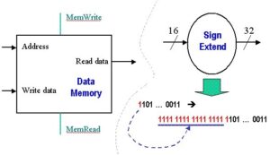
Figure 2. Schematic diagram of Data Memory and Sign Extender, adapted from [Maf01].
R-format Datapath
Implementation of the datapath for R-format instructions is fairly straightforward – the register file and the ALU are all that is required. The ALU accepts its input from the DataRead ports of the register file, and the register file is written to by the ALUresult output of the ALU, in combination with the RegWrite signal.
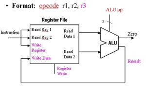
Figure 3. Schematic diagram R-format instruction datapath, adapted from [Maf01].
Load/Store Datapath
The load/store datapath uses instructions such as lw $t1, offset($t2), where offset denotes a memory address offset applied to the base address in register $t2. The lw instruction reads from memory and writes into register $t1. The sw instruction reads from register $t1 and writes into memory. In order to compute the memory address, the MIPS ISA specification says that we have to sign-extend the 16-bit offset to a 32-bit signed value. This is done using the sign extender shown in Figure 2.
The load/store datapath is illustrated in Figure 4, and performs the following actions in the order given:
- Register Access takes input from the register file, to implement the instruction, data, or address fetch step of the fetch-decode-execute cycle.
- Memory Address Calculation decodes the base address and offset, combining them to produce the actual memory address. This step uses the sign extender and ALU.
- Read/Write from Memory takes data or instructions from the data memory, and implements the first part of the execute step of the fetch/decode/execute cycle.
- Write into Register File puts data or instructions into the data memory, implementing the second part of the execute step of the fetch/decode/execute cycle.
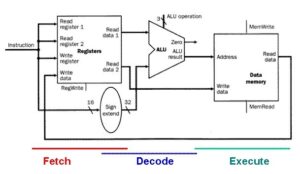
Figure 4. Schematic diagram of the Load/Store instruction datapath. Note that the execute step also includes writing of data back to the register file, which is not shown in the figure, for simplicity [MK98].
The load/store datapath takes operand #1 (the base address) from the register file, and signextends the offset, which is obtained from the instruction input to the register file. The signextended offset and the base address are combined by the ALU to yield the memory address, which is input to the Address port of the data memory. The MemRead signal is then activated, and the output data obtained from the ReadData port of the data memory is then written back to the Register File using its WriteData port, with RegWrite asserted.
Branch/Jump Datapath
The branch datapath (jump is an unconditional branch) uses instructions such as beq $t1, $t2, offset, where offset is a 16-bit offset for computing the branch target address via PC-relative addressing. The beq instruction reads from registers $t1 and $t2, then compares the data obtained from these registers to see if they are equal. If equal, the branch is taken. Otherwise, the branch is not taken.
By taking the branch, the ISA specification means that the ALU adds a sign-extended offset to the program counter (PC). The offset is shifted left 2 bits to allow for word alignment (since 22 = 4, and words are comprised of 4 bytes). Thus, to jump to the target address, the lower 26 bits of the PC are replaced with the lower 26 bits of the instruction shifted left 2 bits.
The branch instruction datapath is illustrated in Figure 4.9, and performs the following actions in the order given:
- Register Access takes input from the register file, to implement the instruction fetch or data fetch step of the fetch-decode-execute cycle.
- Calculate Branch Target – Concurrent with ALU #1’s evaluation of the branch condition, ALU #2 calculates the branch target address, to be ready for the branch if it is taken. This completes the decode step of the fetch-decode-execute cycle.
- Evaluate Branch Condition and Jump to BTA or PC+4 uses ALU #1 in Figure 5, to determine whether or not the branch should be taken. Jump to BTA or PC+4 uses control logic hardware to transfer control to the instruction referenced by the branch target address. This effectively changes the PC to the branch target address, and completes the execute step of the fetch-decode-execute cycle.

Figure 5. Schematic diagram of the Branch instruction datapath. Note that, unlike the Load/Store datapath, the execute step does not include writing of results back to the register file [MK98].
The branch datapath takes operand #1 (the offset) from the instruction input to the register file, then sign-extends the offset. The sign-extended offset and the program counter (incremented by 4 bytes to reference the next instruction after the branch instruction) are combined by ALU #1 to yield the branch target address. The operands for the branch condition to evaluate are concurrently obtained from the register file via the ReadData ports, and are input to ALU #2, which outputs a one or zero value to the branch control logic.
MIPS has the special feature of a delayed branch, that is, instruction Ib which follows the branch is always fetched, decoded, and prepared for execution. If the branch condition is false, a normal branch occurs. If the branch condition is true, then Ib is executed. One wonders why this extra work is performed – the answer is that delayed branch improves the efficiency of pipeline execution. Also, the use of branch-not-taken (where Ib is executed) is sometimes the common case.
Single-Cycle and Multicycle Datapaths
A single-cycle datapath executes in one cycle all instructions that the datapath is designed to implement. This clearly impacts CPI in a beneficial way, namely, CPI = 1 cycle for all instructions. In this section, we first examine the design discipline for implementing such a datapath using the hardware components and instruction-specific datapaths developed in previous section. Then, we discover how the performance of a single-cycle datapath can be improved using a multi-cycle implementation.
Single Datapaths
Let us begin by constructing a datapath with control structures taken from the results of previous section. The simplest way to connect the datapath components developed in the former section is to have them all execute an instruction concurrently, in one cycle. As a result, no datapath component can be used more than once per cycle, which implies duplication of components. To make this type of design more efficient without sacrificing speed, we can share a datapath component by allowing the component to have multiple inputs and outputs selected by a multiplexer.
The key to efficient single-cycle datapath design is to find commonalities among instruction types. For example, the R-format MIPS instruction datapath of Figure 3 and the load/store datapath of Figure 4 have similar register file and ALU connections. However, the following differences can also be observed:
- The second ALU input is a register (R-format instruction) or a signed-extended lower 16 bits of the instruction (e.g., a load/store offset).
- The value written to the register file is obtained from the ALU (R-format instruction) or memory (load/store instruction).
These two datapath designs can be combined to include separate instruction and data memory, as shown in Figure 6. The combination requires an adder and an ALU to respectively increment the PC and execute the R-format instruction.
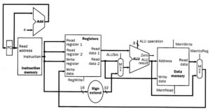
Figure 6. Schematic diagram of a composite datapath for R-format and load/store instructions [MK98].
Adding the branch datapath to the datapath illustrated in Figure 5 produces the augmented datapath shown in Figure 7. The branch instruction uses the main ALU to compare its operands and the adder computes the branch target address. Another multiplexer is required to select either the next instruction address (PC + 4) or the branch target address to be the new value for the PC.
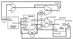
Figure 7. Schematic diagram of a composite datapath for R-format, load/store, and branch instructions [MK98].
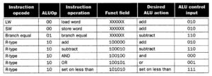
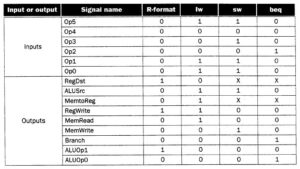
ALU Control. Given the simple datapath shown in Figure 7, we next add the control unit. Control accepts inputs (called control signals) and generates (a) a write signal for each state element, (b) the control signals for each multiplexer, and (c) the ALU control signal. The ALU has three control signals, as shown in Table 1, below.
Table 1. ALU control codes
ALU Control Input Function
—————— ————
000 and
001 or
010 add
- sub
- slt
The ALU is used for all instruction classes, and always performs one of the five functions in the right-hand column of Table 1. For branch instructions, the ALU performs a subtraction, whereas R-format instructions require one of the ALU functions. The ALU is controlled by two inputs: (1) the opcode from a MIPS instruction (six most significant bits), and (2) a two-bit control field (which Patterson and Hennesey call ALUop). The ALUop signal denotes whether the operation should be one of the following:
ALUop Input Operation
————- ————-
- load/store
- beq
10 determined by opcode
The output of the ALU control is one of the 3-bit control codes shown in the left-hand column of Table 4.1. In Table 2, we show how to set the ALU output based on the instruction opcode and the ALUop signals. Later, we will develop a circuit for generating the ALUop bits. We call this approach multi-level decoding — main control generates ALUop bits, which are input to ALU control. The ALU control then generates the three-bit codes shown in Table 1.
The advantage of a hierarchically partitioned or pipelined control scheme is realized in reduced hardware (several small control units are used instead of one large unit). This results in reduced hardware cost, and can in certain instances produce increased speed of control. Since the control unit is critical to datapath performance, this is an important implementational step.
Recall that we need to map the two-bit ALUop field and the six-bit opcode to a three-bit ALU control code. Normally, this would require 2(2 + 6) = 256 possible combinations, eventually expressed as entries in a truth table. However, only a few opcodes are to be implemented in the ALU designed herein. Also, the ALU is used only when ALUop = 102. Thus, we can use simple logic to implement the ALU control, as shown in terms of the truth table illustrated in Table 2.
Table 2. ALU control bits as a function of ALUop bits and opcode bits [MK98].
In this table, an “X” in the input column represents a “don’t-care” value, which indicates that the output does not depend on the input at the i-th bit position. The preceding truth table can be optimized and implemented in terms of gates.
Main Control Unit. The first step in designing the main control unit is to identify the fields of each instruction and the required control lines to implement the datapath shown in Figure 7. Recalling the three MIPS instruction formats (R, I, and J), shown as follows:
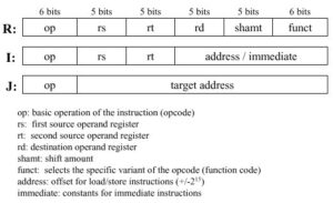
Observe that the following always apply:
- Bits 31-26: opcode – always at this location
- Bits 25-21 and 20-16: input register indices – always at this location
Additionally, we have the following instruction-specific codes due to the regularity of the MIPS instruction format:
- Bits 25-21: base register for load/store instruction – always at this location
- Bits 15-0: 16-bit offset for branch instruction – always at this location
- Bits 15-11: destination register for R-format instruction – always at this location
- Bits 20-16: destination register for load/store instruction – always at this location
Note that the different positions for the two destination registers implies a selector (i.e., a mux) to locate the appropriate field for each type of instruction. Given these contraints, we can add to the simple datapath thus far developed instruction labels and an extra multiplexer for the WriteReg input of the register file, as shown in Figure 8.
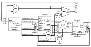
Figure 8. Schematic diagram of composite datapath for R-format, load/store, and branch instructions (from Figure 4.11) with control signals and extra multiplexer for WriteReg signal generation [MK98].
Here, we see the seven-bit control lines (six-bit opcode with one-bit WriteReg signal) together with the two-bit ALUop control signal, whose actions when asserted or deasserted are given as follows:
- RegDst
Deasserted: Register destination number for the Write register is taken from bits 20-16 (rt field) of the instruction
Asserted: Register destination number for the Write register is taken from bits 15-11 (rd field) of the instruction
- RegWrite
Deasserted: No action
Asserted: Register on the WriteRegister input is written with the value on the WriteData input
- ALUSrc
Deasserted: The second ALU operand is taken from the second register file output (ReadData 2)
Asserted: the second alu operand is the sign-extended, lower 16 bits of the instruction
- PCSrc
Deasserted: PC is overwritten by the output of the adder (PC + 4)
Asserted: PC overwritten by the branch target address
- MemRead
Deasserted: No action
Asserted: Data memory contents designated by address input are present at the ReadData output
- MemWrite
Deasserted: No action
Asserted: Data memory contents designated by address input are present at the WriteData input
- RegWrite
Deasserted: The value present at the WriteData input is output from the ALU
Asserted: The value present at the register WriteData input is taken from data memory
Given only the opcode, the control unit can thus set all the control signals except PCSrc, which is only set if the instruction is beq and the Zero output of the ALu used for comparison is true. PCSrc is generated by and-ing a Branch signal from the control unit with the Zero signal from the ALU. Thus, all control signals can be set based on the opcode bits. The resultant datapath and its signals are shown in detail in Figure 9.
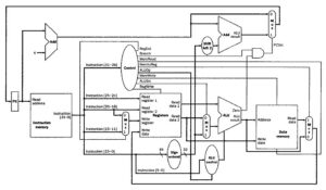
Figure 9. Schematic diagram of composite datapath for R-format, load/store, and branch instructions (from Figure 4.12) with control signals illustrated in detail [MK98].
We next examine functionality of the datapath illustrated in 4.13, for the three major types of instructions, then discuss how to augment the datapath for a new type of instruction.
Datapath Operation
Recall that there are three MIPS instruction formats — R, I, and J. Each instruction causes slightly different functionality to occur along the datapath, as follows.
R-format Instruction Execution of an R-format instruction (e.g., add $t1, $t0, $t1) using the datapath developed in Section 4.3.1 involves the following steps:
- Fetch instruction from instruction memory and increment PC
- Input registers (e.g., $t0 and $t1) are read from the register file
- ALU operates on data from register file using the funct field of the MIPS instruction (Bits 5-0) to help select the ALU operation
- Result from ALU written into register file using bits 15-11 of instruction to select the destination register (e.g., $t1).
Note that this implementational sequence is actually combinational, becuase of the single-cycle assumption. Since the datapath operates within one clock cycle, the signals stabilize approximately in the order shown in Steps 1-4, above.
Load/Store Instruction Execution of a load/store instruction (e.g., lw $t1, offset($t2)) using the datapath developed in previous section involves the following steps:
- Fetch instruction from instruction memory and increment PC
- Read register value (e.g., base address in $t2) from the register file
- ALU adds the base address from register $t2 to the sign-extended lower 16 bits of the instruction (i.e., offset)
- Result from ALU is applied as an address to the data memory
- Data retrieved from the memory unit is written into the register file, where the register index is given by $t1 (Bits 20-16 of the instruction).
Branch Instruction. Execution of a branch instruction (e.g., beq $t1, $t2, offset) using the datapath developed in previous Section involves the following steps:
- Fetch instruction from instruction memory and increment PC
- Read registers (e.g., $t1 and $t2) from the register file. The adder sums PC + 4 plus sign-extended lower 16 bits of offset shifted left by two bits, thereby producing the branch target address (BTA).
- ALU subtracts contents of $t1 minus contents of $t2. The Zero output of the ALU directs which result (PC+4 or BTA) to write as the new PC.
Final Control Design. Now that we have determined the actions that the datapath must perform to compute the three types of MIPS instructions, we can use the information in Table 4.3 to describe the control logic in terms of a truth table. This truth table (Table 4.3) is optimized as to yield the datapath control circuitry.
Table 3. ALU control bits as a function of ALUop bits and opcode bits [MK98].
Extended Control for New Instructions
The jump instruction provides a useful example of how to extend the single-cycle datapath developed in previous section, to support new instructions. Jump resembles branch (a conditional form of the jump instruction), but computes the PC differently and is unconditional. Identical to the branch target address, the lowest two bits of the jump target address (JTA) are always zero, to preserve word alignment. The next 26 bits are taken from a 26-bit immediate field in the jump instruction (the remaining six bits are reserved for the opcode). The upper four bits of the JTA are taken from the upper four bits of the next instruction (PC + 4). Thus, the JTA computed by the jump instruction is formatted as follows:
- Bits 31-28: Upper four bits of (PC + 4)
- Bits 27-02: Immediate field of jump instruction
- Bits 01-00: Zero (002)
The jump is implemented in hardware by adding a control circuit to Figure 9, which is comprised of:
- An additional multiplexer, to select the source for the new PC value. To cover all cases, this source is PC+4, the conditional BTA, or the JTA.
- An additional control signal for the new multiplexer, asserted only for a jump instruction (opcode = 2).
The resulting augmented datapath is shown in Figure 10.
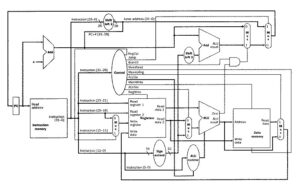
Figure 10. Schematic diagram of composite datapath for R-format, load/store, branch, and jump instructions, with control signals labelled [MK98].
Limitations of the Single-Cycle Datapath
The single-cycle datapath is not used in modern processors, because it is inefficient. The critical path (longest propagation sequence through the datapath) is five components for the load instruction. The cycle time tc is limited by the settling time ts of these components. For a circuit with no feedback loops, tc > 5ts. In practice, tc = 5kts, with large proportionality constant k, due to feedback loops, delayed settling due to circuit noise, etc. Additionally, it is possible to compute the required execution time for each instruction class from the critical path information. The result is that the Load instruction takes 5 units of time, while the Store and R-format instructions take 4 units of time. All the other types of instructions that the datapath is designed to execute run faster, requiring three units of time.
The problem of penalizing addition, subtraction, and comparison operations to accomodate loads and stores leads one to ask if multiple cycles of a much faster clock could be used for each part of the fetch-decode-execute cycle. In practice, this technique is employed in CPU design and implementation, as discussed in the following sections on multicycle datapath design. In Section 5, we will show that datapath actions can be interleaved in time to yield a potentially fast implementation of the fetch-decode-execute cycle that is formalized in a technique called pipelining.
Multicycle Datapath Design
In the previous sections, we designed a single-cycle datapath by (1) grouping instructions into classes, (2) decomposing each instruction class into constituent operations, and (3) deriving datapath components for each instruction class that implemented these operations. In this section, we use the single-cycle datapath components to create a multi-cycle datapath, where each step in the fetch-decode-execute sequence takes one cycle. This approach has two advantages over the single-cycle datapath:
- Each functional unit (e.g., Register File, Data Memory, ALU) can be used more than once in the course of executing an instruction, which saves hardware (and, thus, reduces cost); and
- Each instruction step takes one cycle, so different instructions have different execution times. In contrast, the single-cycle datapath that we designed previously required every instruction to take one cycle, so all the instructions move at the speed of the slowest.
We next consider the basic differences between single-cycle and multi-cycle datapaths.
Cursory Analysis. Figure 11 illustrates a simple multicycle datapath. Observe the following differences between a single-cycle and multi-cycle datapath:
- In the multicycle datapath, one memory unit stores both instructions and data, whereas the single-cycle datapath requires separate instruction and data memories.
- The multicycle datapath uses on ALU, versus an ALU and two adders in the single-cycle datapath, because signals can be rerouted throuh the ALU in a multicycle implementation.
- In the single-cycle implementation, the instruction executes in one cycle (by design) and the outputs of all functional units must stabilize within one cycle. In contrast, the
multicycle implementation uses one or more registers to temporarily store (buffer) the ALU or functional unit outputs. This buffering action stores a value in a temporary register until it is needed or used in a subsequent clock cycle.
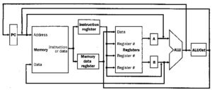
Figure 11. Simple multicycle datapath with buffering registers (Instruction register, Memory data register, A, B, and ALUout) [MK98].
Note that there are two types of state elements (e.g., memory, registers), which are:
- Programmer-Visible (register file, PC, or memory), in which data is stored that is used by subsequent instructions (in a later clock cycle); and
- Additional State Elements(buffer registers), in which data is stored that is used in a later clock cycle of the same instruction.
Thus, the additional (buffer) registers determine (a) what functional units will fit into a given clock cycle and (b) the data required for later cycles involved in executing the current instruction. In the simple implementation presented herein, we assume for purposes of illustration that each clock cycle can accomodate one and only one of the following operations:
- Memory access
- Register file access (two reads or one write)
- ALU operation (arithmetic or logical)
New Registers. As a result of buffering, data produced by memory, register file, or ALU is saved for use in a subsequent cycle. The following temporary registers are important to the multicycle datapath implementation discussed in this section:
- Instruction Register (IR) saves the data output from the Text Segment of memory for a subsequent instruction read;
- Memory Data Register (MDR) saves memory output for a data read operation;
- A and B Registers (A,B) store ALU operand values read from the register file; and ALU Output Register (ALUout) contains the result produced by the ALU.
The IR and MDR are distinct registers because some operations require both instruction and data in the same clock cycle. Since all registers except the IR hold data only between two adjacent clock cycles, these registers do not need a write control signal. In contrast, the IR holds an instruction until it is executed (multiple clock cycles) and therefor requires a write control signal to protect the instruction from being overwritten before its execution has been completed.
New Muxes. We also need to add new multiplexers and expand existing ones, to implement sharing of functional units. For example, we need to select between memory address as PC (for a load instruction) or ALUout (for load/store instructions). The muxes also route to one ALU the many inputs and outputs that were distributed among the several ALUs of the single-cycle datapath. Thus, we make the following additional changes to the single-cycle datapath:
- Add a multiplexer to the first ALU input, to choose between (a) the A register as input (for R- and I-format instructions) , or (b) the PC as input (for branch instructions).
- On the second ALU, the input is selected by a four-way mux (two control bits). The two additional inputs to the mux are (a) the immediate (constant) value 4 for incrementing the PC and (b) the sign-extended offset, shifted two bits to preserve alignment, which is used in computing the branch target address.
The details of these muxes are shown in Figure 12. By adding a few registers (buffers) and muxes (inexpensive widgets), we halve the number of memory units (expensive hardware) and eliminate two adders (more expensive hardware).
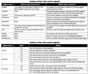
New Control Signals. The datapath shown in Figure 12 is multicycle, since it uses multiple cycles per instruction. As a result, it will require different control signals than the single-cycle datapath, as follows:
- Write Control Signals for the IR and programmer-visible state units Read Control Signal for the memory; and Control Lines for the muxes.
It is advantageous that the ALU control from the single-cycle datapath can be used as-is for the multicycle datapath ALU control. However, some modifications are required to support branches and jumps. We describe these changes as follows.
Branch and Jump Instruction Support. To implement branch and jump instructions, one of three possible values is written to the PC:
- ALU output = PC + 4, to get the next instruction during the instruction fetch step (to do this, PC + 4 is written directly to the PC)
- Register ALUout, which stores the computed branch target address.
- Lower 26 bits (offset) of the IR, shifted left by two bits (to preserve alignment) and concatenated with the upper four bits of PC+4, to form the jump target address.
The PC is written unconditionally (jump instruction) or conditionally (branch), which implies two control signals – PCWrite and PCWriteCond. From these two signals and the Zero output of the ALU, we derive the PCWrite control signal, via the following logic equation:
PCWriteControl = (ALUZero and PCWriteCond) or PCWrite,
where (a) ALUZero indicates if two operands of the beq nstruction are equal and (b) the result of (ALUZero and PCWriteCond) determines whether the PC should be written during a conditional branch. We call the latter the branch taken condition. Figure 4.16 shows the resultant multicycle datapath and control unit with new muxes and corresponding control signals. Table 4.4 illustrates the control signals and their functions.
Multicycle Datapath and Instruction Execution
Given the datapath illustrated in Figure 12, we examine instruction execution in each cycle of the datapath. The implementational goal is balancing of the work performed per clock cycle, to minimize the average time per cycle across all instructions. For example, each step would contain one of the following:
- ALU operation
- Register file access (two reads or one write)
- Memory access (one read or one write)
Thus, the cycle time will be equal to the maximum time required for any of the preceding operations.
Note: Since (a) the datapath is designed to be edge-triggered and (b) the outputs of ALU, register file, or memory are stored in dedicated registers (buffers), we can continue to read the value stored in a dedicated register. The new value, output from ALU, register file, or memory, is not available in the register until the next clock cycle.
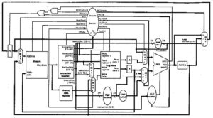
Figure 12. MIPS multicycle datapath [MK98].
Table 4. Multicycle datapath control signals and their functions [MK98].
In the multicycle datapath, all operations within a clock cycle occur in parallel, but successive steps within a given instruction operate sequentially. Several implementational issues present that do not confound this view, but should be discussed. One must distinguish between (a) reading/writing the PC or one of the buffer registers, and (b) reads/writes to the register file. Namely, I/O to the PC or buffers is part of one clock cycle, i.e., we get this essentially “for free” because of the clocking scheme and hardware design. In contrast, the register file has more complex hardware and requires a dedicated clock cycle for its circuitry to stabilize.
We next examine multicycle datapath execution in terms of the fetch-decode-execute sequence.
Instruction Fetch. In this first cycle that is common to all instructions, the datapath fetches an instruction from memory and computes the new PC (address of next instruction in the program sequence), as represented by the following pseudocode:
IR = Memory[PC] # Put contents of Memory[PC] in Instr.Register
PC = PC + 4 # Increment the PC by 4 to preserve alignment
Where, IR denotes the instruction register.
The PC is sent (via control circuitry) as an address to memory. The memory hardware performs a read operation and control hardware transfers the instruction at Memory[PC] into the IR, where it is stored until the next instruction is fetched. Then, the ALU increments the PC by four to preserve word alighment. The incremented (new) PC value is stored back into the PC register by setting PCSource = 00 and asserting PCWrite. Fortunately, incrementing the PC and performing the memory read are concurrent operations, since the new PC is not required (at the earliest) until the next clock cycle.
Instruction Decode and Data Fetch. Included in the multicycle datapath design is the assumption that the actual opcode to be executed is not known prior to the instruction decode step. This is reasonable, since the new instruction is not yet available until completion of instruction fetch and has thus not been decoded.
As a result of not knowing what operation the ALU is to perform in the current instruction, the datapath must execute only actions that are:
- Applicable to all instructions and
- Not harmful to any
Therefore, given the rs and rt fields of the MIPS instruction format, we can suppose (harmlessly) that the next instruction will be R-format. We can thus read the operands corresponding to rs and rt from the register file. If we don’t need one or both of these operands, that is not harmful. Otherwise, the register file read operation will place them in buffer registers A and B, which is also not harmful.
Another action the datapath can perform is computation of the branch target address using the ALU, since this is the instruction decode step and the ALU is not yet needed for instruction execution. If the instruction that we are decoding in this step is not a branch, then no harm is done – the BTA is stored in ALUout and nothing further happens to it.
We can perform these preparatory actions because of the <i.regularity< i=””> of MIPS instruction formats. The result is represented in pseudocode, as follows: </i.regularity<>
- = RegFile[IR[25:21]] # First operand = Bits 25-21 of instruction
- = RegFile[IR[20:16]] # Second operand = Bits 25-21 of instruction
ALUout = PC + SignExtend(IR[15:0]) << 2 ; # Compute BTA
Where, “x << n” denotes x shifted left by n bits.
Instruction Execute, Address Computation, or Branch Completion. In this cycle, we know what the instruction is, since decoding was completed in the previous cycle. The instruction opcode determines the datapath operation, as in the single-cycle datapath. The ALU operates upon the operands prepared in the decode/data-fetch step, performing one of the following actions:
- Memory Reference: ALUout = A + SignExtend(IR[15:0])
The ALU constructs the memory address from the base address (stored in A) and the offset (taken from the low 16 bits of the IR). Control signals are set as described on p. 387 opf the textbook.
- R-format Instruction: ALUout = A op B
The ALU takes its inputs from buffer registers A and B and computes a result according to control signals specified by the instruction opcode, function field, and control signals ALUop = 10. The control signals are further described on p. 387 of the textbook.
- Branch: if (A == B) then PC = ALUout
In branch instructions, the ALU performs the comparison between the contents of registers A and B. If A = B, then the Zero output of the ALU is asserted, the PC is updated (overwritten) with (1) the BTA computed in the preceding step, then (2) the ALUout value. If the branch is not taken, then the PC+4 value computed during instruction fetch is used. This covers all possibilities by using for the BTA the value most recently written into the PC. Salient hardware control actions are discussed on p. 387 of the textbook.
- Jump: PC = PC[31:28] || (IR[25:0] << 2)
Here, the PC is replaced by the jump target address, which does not need the ALU be computed, but can be formed in hardware as described on p. 387 of the textbook.
Memory Access or R-format Instruction Completion. In this cycle, a load-store instruction accesses memory and an R-format instruction writes its result (which appears at ALUout at the end of the previous cycle), as follows:
MDR = Memory[ALUout] # Load
Memory[ALUout] = B # Store where MDR denotes the memory data register.
For an R-format completion, where
Reg[IR[15:11]] = ALUout # Write ALU result to register file
the data to be loaded was stored in the MDR in the previous cycle and is thus available for this cycle. The rt field of the MIPS instruction format (Bits 20-16) has the register number, which is applied to the input of the register file, together with RegDst = 0 and an asserted RegWrite signal.
0 Comments