Part 7: Intel 8086 16-Bit Microprocessor Architecture: BIU, EU, Segmented Memory, and Instruction Pipelining
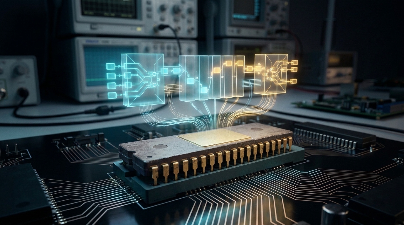
The Genesis of the x86 Architecture
Launched in 1978, the Intel 8086 represents one of the most consequential milestones in computer history. As a 16-bit microprocessor with a 20-bit address bus capable of accessing 1 Megabyte ($1,048,576$ bytes) of memory, the 8086 introduced instruction pipelining, memory segmentation, and a dual-processing unit topology that gave birth to the enduring x86 instruction set. In Part 7, we analyze the Bus Interface Unit, the Execution Unit, physical address calculation, and the fundamental differences between the 8085 and 8086.
1. Two Independent Functional Units: BIU and EU
In earlier processors like the 8085, the CPU executed instructions strictly serially: it fetched an instruction from memory, waited while internal logic decoded and executed it, and only then fetched the next opcode. During execution, the external memory bus remained idle.
The 8086 fundamentally solved this bus latency bottleneck by dividing its silicon architecture into two asynchronous, independently functioning units: the Bus Interface Unit (BIU) and the Execution Unit (EU).
Bus Interface Unit (BIU)
Bus OperationsThe BIU handles all data and address transactions with external memory and I/O peripherals. While the EU is busy executing previously fetched instructions, the BIU proactively fetches ahead up to 6 bytes of subsequent instructions from code memory and stores them in its internal FIFO queue.
- 6-Byte Instruction Prefetch Queue: Implements first-in, first-out hardware pipelining.
- Segment Registers: Code Segment (CS), Data Segment (DS), Stack Segment (SS), Extra Segment (ES).
- Instruction Pointer (IP): 16-bit register tracking the offset of the next opcode.
- Dedicated 20-bit Address Adder: Calculates physical memory addresses.
Execution Unit (EU)
Computation EngineThe EU has no direct connection to the external system bus. It fetches instructions exclusively from the output of the BIU's 6-byte queue, decodes them, and executes them over its internal 16-bit data paths.
- 16-bit ALU: Performs arithmetic (including hardware 16-bit multiply/divide) and logic.
- General Purpose Registers: AX, BX, CX, DX (can be split into 8-bit halves: AH/AL, BH/BL, CH/CL, DH/DL).
- Pointers & Index Registers: Stack Pointer (SP), Base Pointer (BP), Source Index (SI), Destination Index (DI).
- 16-bit Flag Register: 9 active status and control flip-flops.
2. Instruction Pipelining in the 8086
The 6-byte FIFO queue in the BIU forms an elementary two-stage instruction pipeline:
- Whenever at least 2 bytes in the queue become empty and the EU does not require the system bus for operand memory access, the BIU automatically executes an instruction prefetch cycle.
- When the EU completes an instruction, it instantly fetches the next opcode from the front of the queue in zero clock cycles, eliminating the traditional opcode fetch delay.
- Pipeline Stall / Branch Penalty: If a jump (
JMP), conditional branch (JZ,JNZ), call (CALL), or interrupt occurs, the target address lies outside the sequential queue. The entire 6-byte queue must be invalidated (flushed), and the BIU must initiate a full bus cycle to fetch from the new target address.
3. Memory Segmentation & 20-Bit Physical Address Calculation
The 8086 has a 20-bit address bus, enabling access to $2^{20} = 1,048,576\text{ bytes} = 1\text{ MB}$ of memory. However, all internal registers (including IP, SP, SI, DI) are only 16 bits wide ($2^{16} = 64\text{ KB}$).
To bridge this disparity, Intel adopted Memory Segmentation. The 1 MB physical memory space is divided into logical segments of up to 64 KB each. At any moment, the processor can actively address four distinct 64 KB segments:
- Code Segment (CS): Contains program instructions. Paired with Instruction Pointer (
CS:IP). - Data Segment (DS): Houses global and static program variables. Paired with general offsets (
DS:SI,DS:BX). - Stack Segment (SS): Stores return addresses, passed parameters, and local variables. Paired with Stack Pointer (
SS:SP) and Base Pointer (SS:BP). - Extra Segment (ES): Provides auxiliary data storage, particularly for destination strings in string operations (
ES:DI).
Physical Address Generation Formula
To produce the 20-bit physical address placed onto pins $A_0 - A_{19}$, the 16-bit segment base register is shifted left by 4 binary bits (multiplied by 16, or shifted by one hexadecimal digit) and added to the 16-bit offset address:
If Code Segment Register CS =
348AH and Instruction Pointer IP = 4214H:1. Shift CS left by 4 bits (1 hex digit):
348A0H2. Add 16-bit offset from IP:
+ 04214H3. 20-Bit Resulting Physical Address:
= 38AB4H
4. Intel 8085 vs. Intel 8086: Comparative Matrix
| Feature | Intel 8085 | Intel 8086 |
|---|---|---|
| Word Size | 8-bit internal ALU and data registers | 16-bit internal ALU and data registers |
| Address Bus Width | 16-bit (Can address 64 KB memory) | 20-bit (Can address 1 MB memory) |
| External Data Bus | 8-bit bidirectional ($AD_0 - AD_7$) | 16-bit bidirectional ($AD_0 - AD_{15}$) |
| Pipelining / Queue | No pipelining; sequential fetch and execute | Pipelined; 6-byte instruction prefetch FIFO queue |
| Operating Modes | Single mode of operation | Dual modes: Minimum Mode (single CPU) & Maximum Mode (multiprocessor) |
| Hardware Arithmetic | Only addition, subtraction, increment, decrement | Dedicated hardware 16-bit signed/unsigned MUL and DIV |
Summary & Next Step
In Part 8, we analyze the 40-pin DIP layout of the 8086, detail its Minimum Mode versus Maximum Mode pinouts, and survey the comprehensive 8086 instruction set.
Related reading
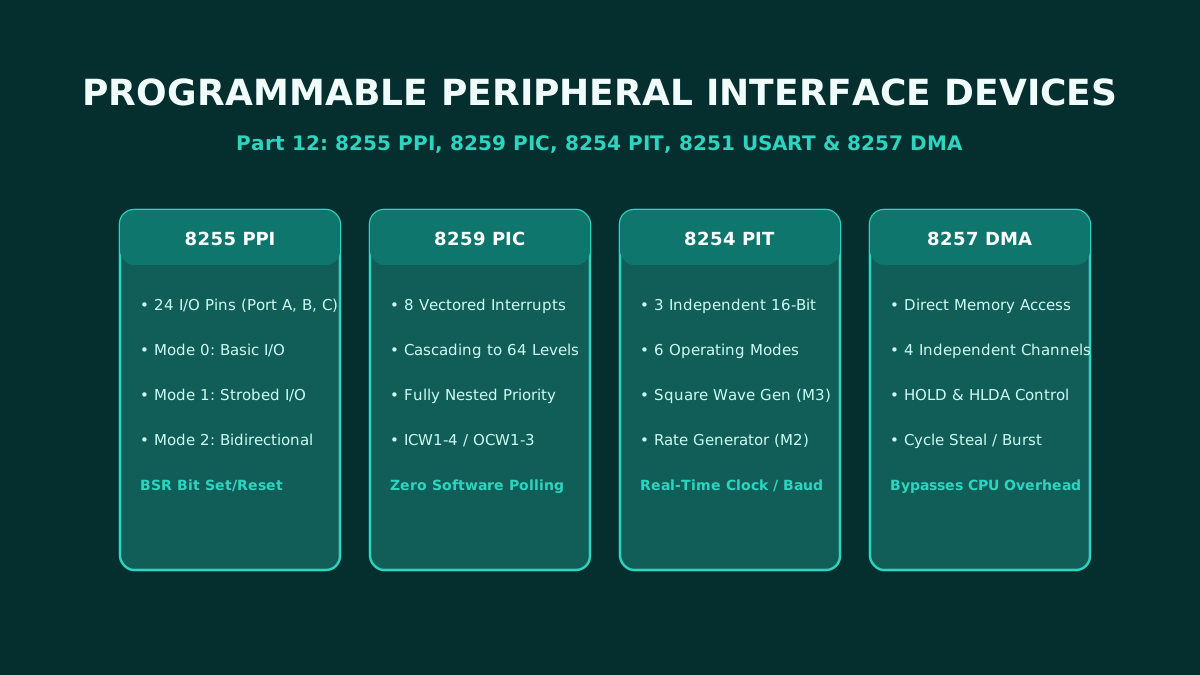
Part 12: Programmable Peripheral Interface ICs: Architecture and Pin Configuration of 8255, 8259, 8254, 8251, and 8257
The ultimate hardware reference for microprocessor peripheral interface adapters: complete architecture, pin configurations, and control word programming for the 8255 PPI, 8259 PIC, 8254 PIT, 8251 USART, and 8257 DMA controller.
By Md. Harun-Or-Roshid
Part 11: Intel 8051 Microcontroller Architecture: Harvard Memory Map, SFRs, and I/O Port Circuits
A master-level architectural analysis of the Intel 8051 microcontroller: Microprocessor vs Microcontroller paradigm, Harvard memory organization, 128-byte internal RAM layout, SFR registers, and internal circuits of Ports 0–3.
By Md. Harun-Or-Roshid
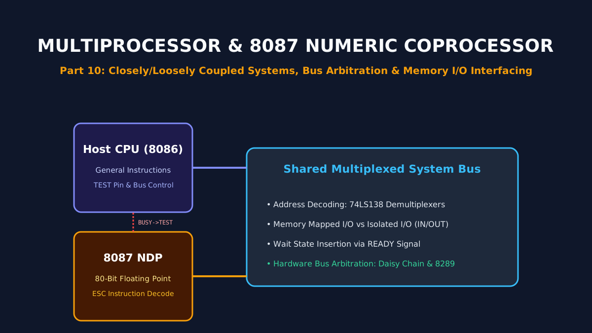
Part 10: Multiprocessor Configurations, 8087 Numeric Coprocessor, and Memory/IO Interfacing
Architectural principles of multiprocessor systems: closely vs loosely coupled topologies, hardware bus arbitration, the Intel 8087 floating-point NDP, and memory-mapped vs isolated I/O interfacing.
By Md. Harun-Or-Roshid
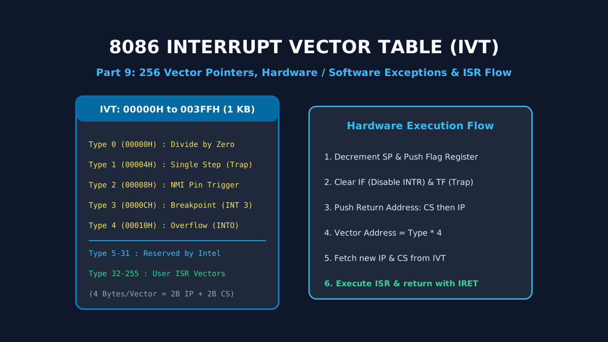
Part 9: Interrupt Structures and Vector Pointer Table in Intel 8086: Hardware, Software, and Exception Handling
A deep dive into 8086 interrupt processing: the 1 KB Interrupt Vector Table (IVT), dedicated Type 0–4 exceptions, hardware NMI/INTR lines, the 6-step interrupt response cycle, and the IRET sequence.
By Md. Harun-Or-Roshid