Part 11: Intel 8051 Microcontroller Architecture: Harvard Memory Map, SFRs, and I/O Port Circuits
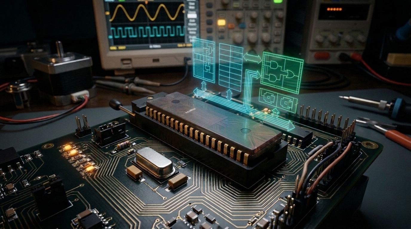
The Monolithic System on a Chip
While microprocessors (such as the 8085 and 8086) require external RAM chips, ROM chips, timer ICs, and programmable I/O ports connected across a printed circuit board to function, a microcontroller integrates all of these essential microcomputer components onto a single monolithic silicon die. Released in 1980, the Intel 8051 defined the architecture of modern embedded control. In Part 11, we explore the Harvard memory architecture, the 128-byte internal RAM layout, Special Function Registers (SFRs), and the delicate transistor-level circuitry of its four bidirectional I/O ports.
1. Microprocessor vs. Microcontroller
| Parameter | Microprocessor (e.g. 8085 / 8086) | Microcontroller (e.g. Intel 8051) |
|---|---|---|
| Silicon Contents | Contains CPU core only (ALU, registers, timing unit). Memory and I/O must be connected externally. | Complete microcomputer on-chip: CPU, RAM, ROM, I/O ports, timers/counters, and UART serial port. |
| Memory Architecture | Von Neumann model (Data and instructions share a common physical address bus and memory space). | Harvard Architecture: Physically separate address spaces for Program Memory (ROM) and Data Memory (RAM). |
| Board Size & Cost | Large PCB footprint; requires multiple bus transceivers, address latches, and external memories. | Extremely compact footprint; low board component count, low system cost, high noise immunity. |
| Bit Manipulation | Limited; requires masking operations with AND/OR to manipulate individual bits. | Extensive Boolean Processor: Direct bit-level instructions (SETB, CLR, CPL, JB, JNB). |
2. 8051 On-Chip Hardware Specifications
4 KB
On-Chip Program ROM
128 B
On-Chip Data RAM
32
Bidirectional I/O Lines (4 Ports)
2 x 16-Bit
Hardware Timers / Counters
3. Internal 128-Byte RAM Structure (00H to 7FH)
The 128 bytes of internal data memory ($00\text{H} - 7\text{FH}$) are partitioned into three distinct functional zones:
1. Four Working Register Banks (00H – 1FH: 32 Bytes)
Contains four switchable register banks (Bank 0, Bank 1, Bank 2, Bank 3). Each bank contains eight 8-bit registers labeled R0 through R7. The active bank is selected by setting or clearing bits $RS_1$ and $RS_0$ in the Program Status Word (PSW). Enables instant context-switching during interrupt service routines without saving registers to stack.
2. Bit-Addressable RAM (20H – 2FH: 16 Bytes / 128 Bits)
These 16 bytes contain 128 individually addressable bits, assigned bit addresses from $00\text{H}$ to $7\text{FH}$. Any individual bit can be tested, set, or cleared in a single instruction (e.g. SETB 05H sets bit 5 of byte 20H).
3. General Purpose Scratchpad RAM (30H – 7FH: 80 Bytes)
General byte-addressable read/write storage used for program variables and runtime data structures. Also houses the 8051 Stack, which grows upward into this space (Stack Pointer SP initializes to $07\text{H}$ on reset).
4. Special Function Registers (SFRs: 80H to FFH)
Addresses $80\text{H}$ to $FF\text{H}$ are reserved for Special Function Registers that configure and monitor on-chip peripherals. Key SFRs include:
- ACC (E0H) & B (F0H): Accumulator and register B used by hardware multiplication (
MUL AB) and division (DIV AB). - PSW (D0H - Program Status Word): Holds CY, AC, F0, RS1, RS0, OV (Overflow), and P (Parity).
- DPTR (82H-83H): 16-bit Data Pointer (DPH and DPL) used to access external code (
MOVC) and external data RAM (MOVX). - TMOD (89H) & TCON (88H): Timer Mode and Timer Control registers managing Timers 0 and 1.
- SCON (98H) & SBUF (99H): Serial Control and Serial Data Buffer for UART communications.
- IE (A8H) & IP (B8H): Interrupt Enable and Interrupt Priority registers.
5. Circuit Architecture of the 4 I/O Ports
Port 0 (Pins 32–39) - True Open-Drain
Port 0 lacks internal pull-up resistors. When used as a general-purpose I/O port, external pull-up resistors (typically $10\,\text{k}\Omega$) must be connected to $+5V$. When accessing external memory, internal control multiplexers automatically configure Port 0 as the time-multiplexed low-order Address/Data bus ($AD_0 - AD_7$), driving high/low with active push-pull FETs.
Port 1 (Pins 1–8) - Dedicated Quasi-Bidirectional I/O
Port 1 features internal pull-up FETs and is exclusively dedicated to general-purpose digital I/O. To configure any pin as an input, software must first write a 1 to the pin's latch.
Port 2 (Pins 21–28) - I/O & High-Order Address Bus
Port 2 includes internal pull-up resistors. It functions as general-purpose I/O or automatically outputs the high-order 8 bits of address ($A_8 - A_{15}$) during external 16-bit memory operations (MOVX @DPTR).
Port 3 (Pins 10–17) - Multifunctional Alternate Pins
In addition to general-purpose quasi-bidirectional I/O with internal pull-ups, every pin of Port 3 serves a critical secondary hardware function:
| Pin | Mnemonic | Alternate Hardware Function |
|---|---|---|
| P3.0 | RXD | Serial data input line for on-chip UART |
| P3.1 | TXD | Serial data output line for on-chip UART |
| P3.2 | INT0# | External hardware interrupt 0 (Active LOW) |
| P3.3 | INT1# | External hardware interrupt 1 (Active LOW) |
| P3.4 | T0 | External clock input for Timer 0 counter |
| P3.5 | T1 | External clock input for Timer 1 counter |
| P3.6 | WR# | External Data Memory Write strobe |
| P3.7 | RD# | External Data Memory Read strobe |
Summary & Next Step
In our final installment, Part 12, we examine the essential Programmable Peripheral Interface (PPI) ICs that connect microprocessors to external hardware: the 8255 PPI, 8259 Priority Interrupt Controller, 8254 Interval Timer, 8251 USART, and 8257 DMA Controller.
Related reading
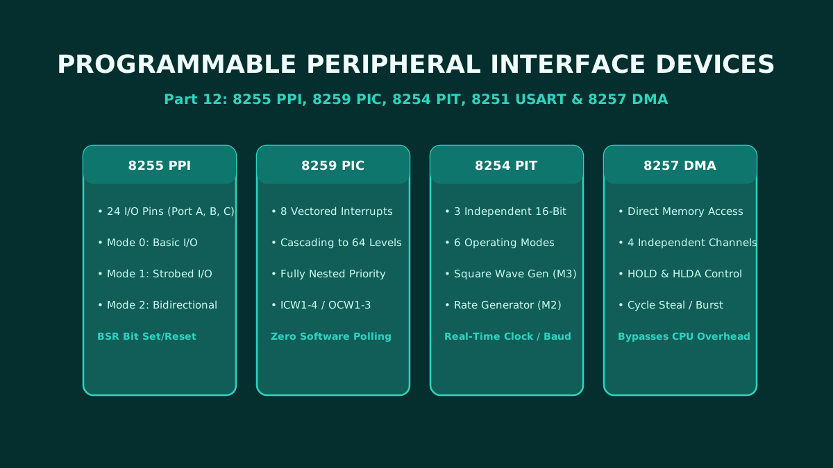
Part 12: Programmable Peripheral Interface ICs: Architecture and Pin Configuration of 8255, 8259, 8254, 8251, and 8257
The ultimate hardware reference for microprocessor peripheral interface adapters: complete architecture, pin configurations, and control word programming for the 8255 PPI, 8259 PIC, 8254 PIT, 8251 USART, and 8257 DMA controller.
By Md. Harun-Or-Roshid
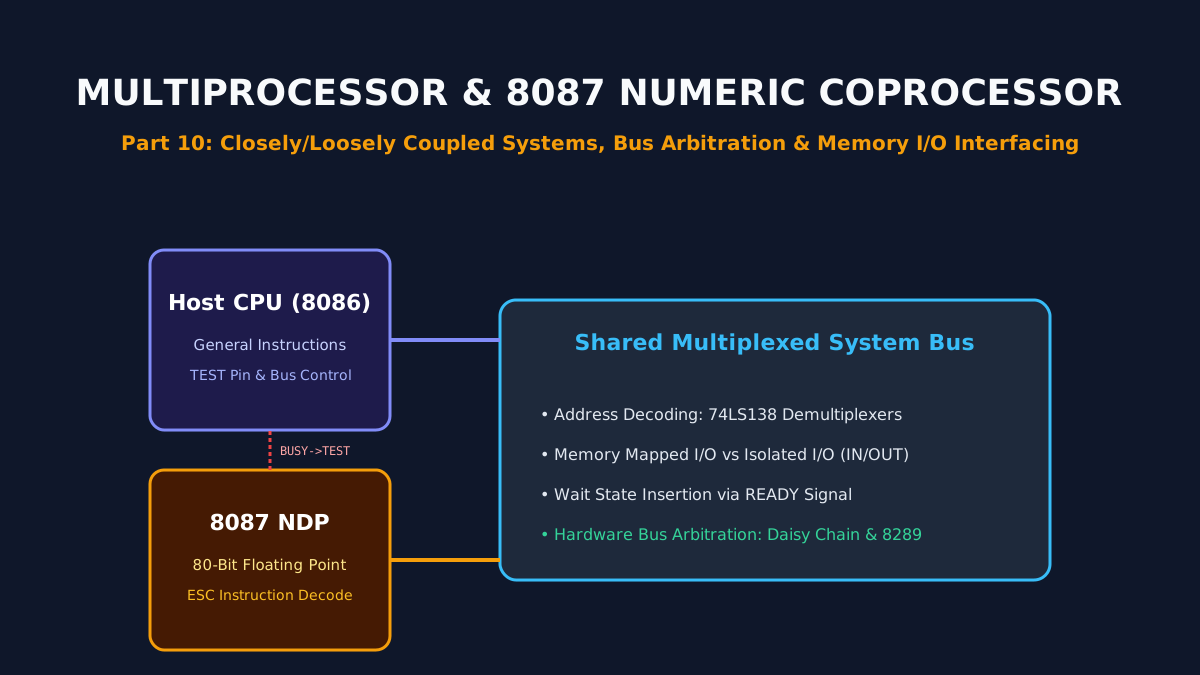
Part 10: Multiprocessor Configurations, 8087 Numeric Coprocessor, and Memory/IO Interfacing
Architectural principles of multiprocessor systems: closely vs loosely coupled topologies, hardware bus arbitration, the Intel 8087 floating-point NDP, and memory-mapped vs isolated I/O interfacing.
By Md. Harun-Or-Roshid
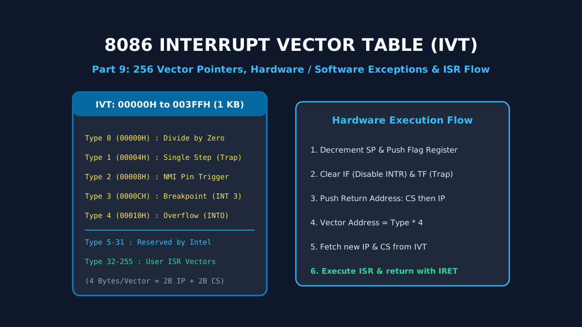
Part 9: Interrupt Structures and Vector Pointer Table in Intel 8086: Hardware, Software, and Exception Handling
A deep dive into 8086 interrupt processing: the 1 KB Interrupt Vector Table (IVT), dedicated Type 0–4 exceptions, hardware NMI/INTR lines, the 6-step interrupt response cycle, and the IRET sequence.
By Md. Harun-Or-Roshid
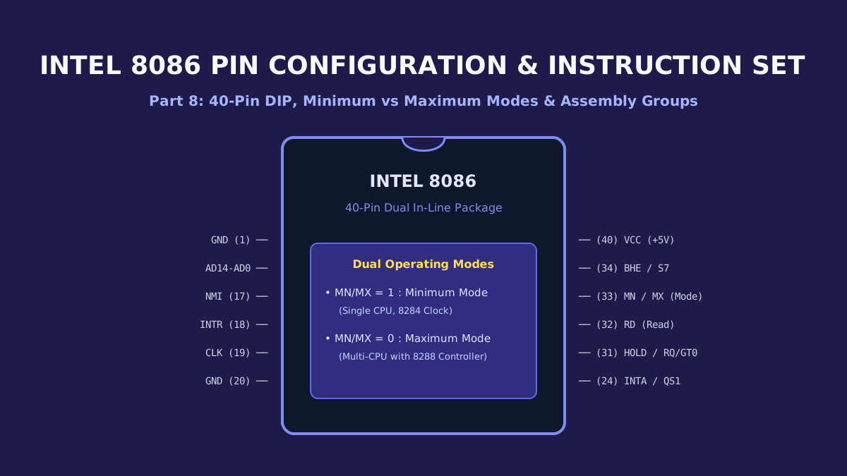
Part 8: Intel 8086 Pin Configuration, Operating Modes (Min/Max), and Comprehensive Instruction Set
Exhaustive hardware guide to the 40-pin Intel 8086: multiplexed address/data pins, Minimum Mode uniprocessor vs Maximum Mode multiprocessor circuits with the 8288 bus controller, and complete instruction set categorization.
By Md. Harun-Or-Roshid