Part 8: Intel 8086 Pin Configuration, Operating Modes (Min/Max), and Comprehensive Instruction Set
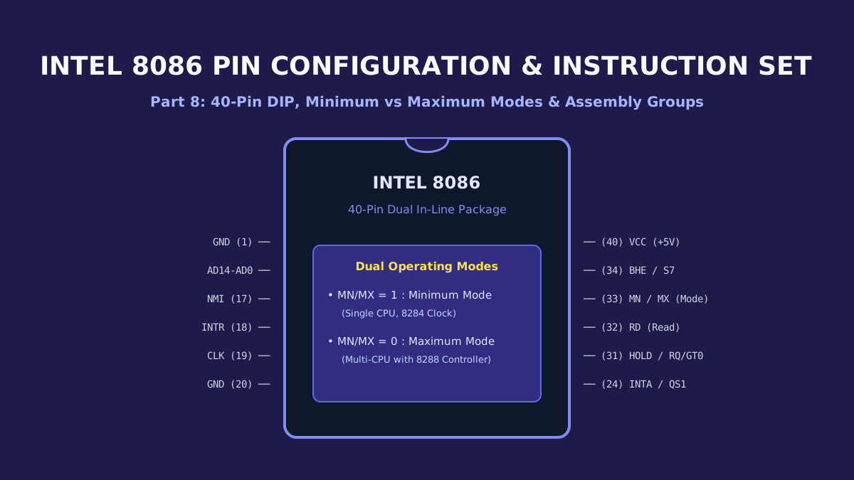
Silicon Pinout & Dual System Modes
Like its predecessor, the Intel 8086 was manufactured in a 40-pin Dual In-Line Package (DIP). However, transmitting a 20-bit address bus and a 16-bit data bus required sophisticated pin-multiplexing and a dual operating mode feature controlled by a single silicon pin: MN/MX#. In Part 8, we examine the 8086 pin functions in Minimum and Maximum modes, explain how external support chips (8284, 8282, 8286, 8288) form complete systems, and categorize the full 8086 instruction set.
1. 40-Pin DIP Pinout Analysis
Multiplexed Address & Data Pins
- $AD_0 - AD_{15}$ (Pins 16-9, 2-8, 39): Multiplexed Address and Data bus. During clock state $T_1$, these pins carry the low-order 16 bits of memory address ($A_0 - A_{15}$). During $T_2 - T_4$, they carry 16-bit bidirectional data ($D_0 - D_{15}$).
- $A_{16}/S_3 - A_{19}/S_6$ (Pins 35-38): Multiplexed upper Address lines and Status signals. During $T_1$, they provide the upper 4 address bits ($A_{16} - A_{19}$) needed to address 1 MB. During $T_2 - T_4$, they output status codes: $S_3$ and $S_4$ identify which segment register is being accessed (00=ES, 01=SS, 10=CS/None, 11=DS); $S_5$ indicates the state of the Interrupt Flag (IF); $S_6$ is permanently LOW.
- $\overline{\text{BHE}}/S_7$ (Pin 34 - Bus High Enable): Used to enable data transfer onto the upper byte of the data bus ($D_8 - D_{15}$). Together with $A_0$, it selects whether the CPU accesses an Even Memory Bank (lower byte), Odd Memory Bank (upper byte), or a full 16-bit word concurrently.
2. Minimum Mode vs. Maximum Mode Operation
Pin 33 is the Mode Select Pin ($MN/\overline{MX}$). Connecting this pin directly to $+5V$ configures the 8086 in Minimum Mode. Grounding it configures the processor in Maximum Mode.
Minimum Mode ($MN/\overline{MX} = 1$)
Single-CPU SystemDesigned for cost-effective single-processor systems. The 8086 directly generates all memory and I/O control strobes from its own pins 24 to 31:
M/IO#: Memory (HIGH) vs I/O (LOW) access.RD#/WR#: Memory and I/O Read and Write strobes.ALE: Address Latch Enable for 8282/74LS373 latches.DEN#: Data Enable (activates 8286 transceivers).DT/R#: Data Transmit/Receive direction control.HOLD/HLDA: Direct DMA bus arbitration pins.
Maximum Mode ($MN/\overline{MX} = 0$)
Multiprocessor SystemRequired when the 8086 is paired with math coprocessors (Intel 8087) or I/O processors (Intel 8089). Pins 24 to 31 are redefined:
S0#, S1#, S2#: Status lines decoded by external 8288 Bus Controller to generate bus control commands.LOCK#: Bus lock strobe; prevents other processors from seizing the bus during critical atomic operations (e.g.LOCK XCHG).QS0, QS1: Queue Status signals telling coprocessors the state of the BIU instruction queue.RQ#/GT0#, RQ#/GT1#: Bidirectional Request/Grant bus arbitration lines.
3. The 8086 Instruction Groups
1. Data Transfer Group
Includes general-purpose moves (MOV), stack pushes/pops (PUSH, POP), register exchange (XCHG), translation table lookup (XLAT), peripheral port I/O (IN, OUT), and address transfer pointers (LEA, LDS, LES).
2. Arithmetic Group
Supports 8-bit and 16-bit addition (ADD, ADC), subtraction (SUB, SBB), hardware multiplication (unsigned MUL, signed IMUL), and division (unsigned DIV, signed IDIV). Includes sign extension instructions (CBW: Byte to Word in AX, CWD: Word to Doubleword in DX:AX) and BCD adjustment (DAA, DAS, AAA, AAM, AAD).
3. String Manipulation Group
Dedicated instructions for high-speed block data processing in memory: MOVSB/MOVSW (Move String), CMPSB/CMPSW (Compare String), SCASB/SCASW (Scan String), LODSB/LODSW (Load String into AX), and STOSB/STOSW (Store AX into String). Can be prefixed with hardware repeat prefixes (REP, REPE/REPZ, REPNE/REPNZ) that decrement the counter register CX until zero, achieving memory block copies at wire speed.
4. Program Execution Control Group
Unconditional and conditional jumps (JMP, JE/JZ, JNE/JNZ, JG/JNLE, JL/JNGE), procedure calls (CALL, RET), loop counter control (LOOP, LOOPZ, LOOPNZ), software interrupts (INT n, INTO), and return from interrupt (IRET).
Summary & Next Step
In Part 9, we examine the 8086 Interrupt Vector Table (IVT), analyzing dedicated hardware interrupts (NMI, INTR), software exceptions (Divide by Zero, Single Step, Breakpoint), and the deterministic 6-step interrupt response cycle.
Related reading
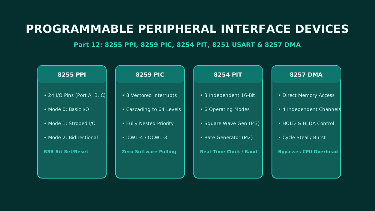
Part 12: Programmable Peripheral Interface ICs: Architecture and Pin Configuration of 8255, 8259, 8254, 8251, and 8257
The ultimate hardware reference for microprocessor peripheral interface adapters: complete architecture, pin configurations, and control word programming for the 8255 PPI, 8259 PIC, 8254 PIT, 8251 USART, and 8257 DMA controller.
By Md. Harun-Or-Roshid
Part 11: Intel 8051 Microcontroller Architecture: Harvard Memory Map, SFRs, and I/O Port Circuits
A master-level architectural analysis of the Intel 8051 microcontroller: Microprocessor vs Microcontroller paradigm, Harvard memory organization, 128-byte internal RAM layout, SFR registers, and internal circuits of Ports 0–3.
By Md. Harun-Or-Roshid
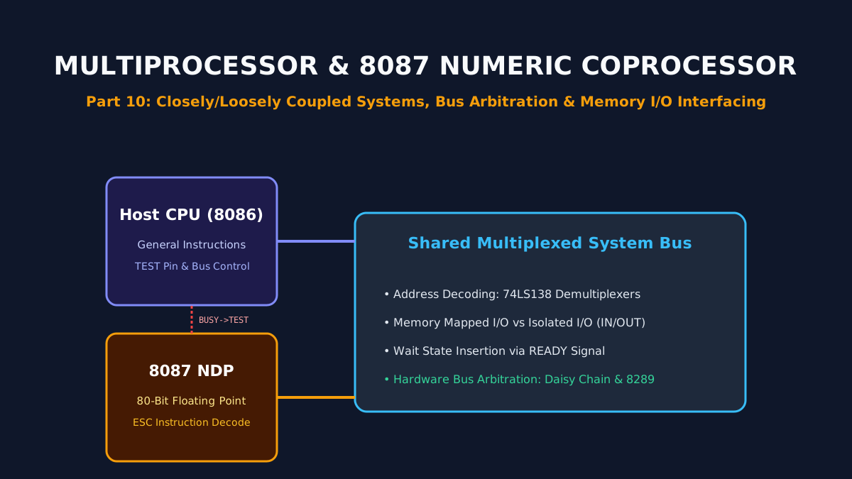
Part 10: Multiprocessor Configurations, 8087 Numeric Coprocessor, and Memory/IO Interfacing
Architectural principles of multiprocessor systems: closely vs loosely coupled topologies, hardware bus arbitration, the Intel 8087 floating-point NDP, and memory-mapped vs isolated I/O interfacing.
By Md. Harun-Or-Roshid
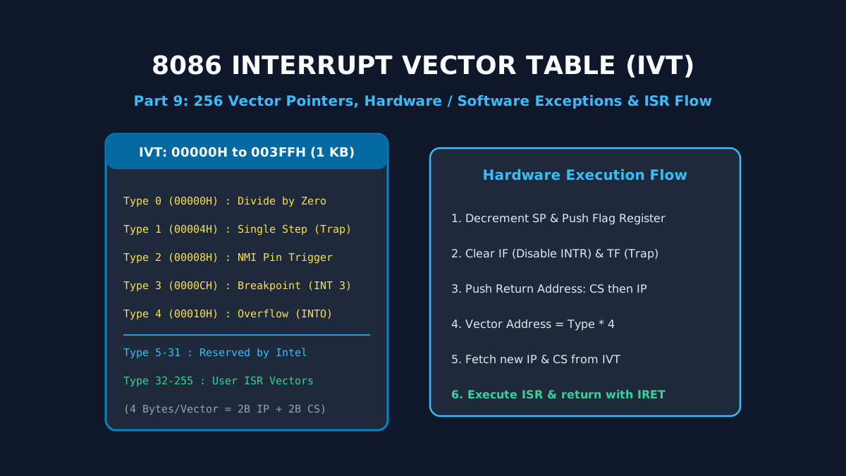
Part 9: Interrupt Structures and Vector Pointer Table in Intel 8086: Hardware, Software, and Exception Handling
A deep dive into 8086 interrupt processing: the 1 KB Interrupt Vector Table (IVT), dedicated Type 0–4 exceptions, hardware NMI/INTR lines, the 6-step interrupt response cycle, and the IRET sequence.
By Md. Harun-Or-Roshid