Part 12: Programmable Peripheral Interface ICs: Architecture and Pin Configuration of 8255, 8259, 8254, 8251, and 8257
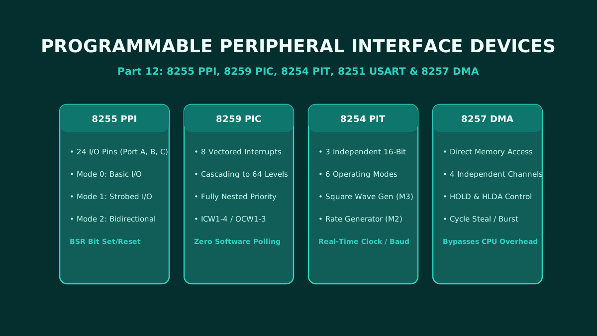
Bridging the CPU to the Physical World
A microprocessor in isolation is merely a fast mathematical engine; it requires specialized peripheral interface adapters to communicate with keyboards, display terminals, analog-to-digital converters, motor actuators, and disk drives. In this culminating installment of our 12-part series, we examine the architecture, pin configurations, operating modes, and control register formats of the classic Intel peripheral family: the 8255 PPI, 8259 PIC, 8254 PIT, 8251 USART, and 8257 DMA Controller.
1. Intel 8255 Programmable Peripheral Interface (PPI)
The 8255 is a general-purpose programmable I/O device configured into 24 I/O pins organized as three 8-bit ports (Port A, Port B, Port C) grouped into Group A and Group B:
8255 Operating Modes
- Mode 0 (Basic Input/Output): Simple unlatched input and latched output on all 24 pins without handshaking signals. Useful for reading DIP switches and driving LED displays.
- Mode 1 (Strobed Input/Output): Handshake data transfer. Port A and Port B function as 8-bit data ports, while pins of Port C generate handshake strobes (
STB#Strobe,IBFInput Buffer Full,INTRInterrupt Request,OBF#Output Buffer Full,ACK#Acknowledge). - Mode 2 (Strobed Bidirectional Bus I/O): Supported exclusively on Port A. Port A acts as an 8-bit bidirectional data bus using 5 pins of Port C for handshaking. Enables master-slave peripheral communication.
- BSR (Bit Set/Reset) Mode: Applies exclusively to Port C. Individual bits of Port C can be set or cleared with a single control word write without affecting the remaining Port C bits. Ideal for generating software pulses and motor control steps.
8255 I/O Control Word Format (Bit D7 = 1)
| Bit | Field | Value = 1 | Value = 0 |
|---|---|---|---|
| D7 | Mode Set Flag | Active (I/O Mode) | BSR Mode (when D7 = 0) |
| D6, D5 | Group A Mode | 00 = Mode 0; 01 = Mode 1; 1X = Mode 2 | - |
| D4 | Port A Direction | Input | Output |
| D3 | Port C Upper (PC7-PC4) | Input | Output |
| D2 | Group B Mode | Mode 1 | Mode 0 |
| D1 | Port B Direction | Input | Output |
| D0 | Port C Lower (PC3-PC0) | Input | Output |
2. Intel 8259 Priority Interrupt Controller (PIC)
The 8259 manages up to 8 vectored priority interrupts on a single chip, cascading up to 64 vectored interrupts across a master-slave configuration (1 Master 8259 + 8 Slave 8259s connected via cascade lines CAS0-CAS2):
Internal Registers
- IRR (Interrupt Request Register): Latches pending interrupt requests on lines $IR_0 - IR_7$.
- ISR (In-Service Register): Tracks which interrupt level is currently being serviced by the CPU.
- IMR (Interrupt Mask Register): 8-bit mask register; setting a bit masks (disables) that specific interrupt line.
- Priority Resolver: Hardware logic that selects the highest-priority unmasked pending interrupt.
Programming Words
Configured via Initialization Command Words (ICW1–ICW4) to set base vector addresses, edge/level triggering, single/cascade mode, and 8085/8086 mode. Runtime priority updates are managed via Operation Command Words (OCW1–OCW3), including End of Interrupt (EOI) commands.
3. Intel 8254 Programmable Interval Timer (PIT)
The 8254 contains three independent 16-bit counters (Counter 0, 1, 2) that decrement from a preloaded count down to zero at clock input frequencies up to 10 MHz. It provides six programmable operational modes:
- Mode 0: Interrupt on Terminal Count (Output drops LOW upon mode load, goes HIGH when counter reaches zero).
- Mode 1: Hardware Retriggerable One-Shot (Generates clean one-shot pulse on GATE trigger).
- Mode 2: Rate Generator (Frequency divider; outputs a single-clock-wide pulse once every $N$ input clock periods).
- Mode 3: Square Wave Generator (Outputs continuous 50% duty cycle square wave; used for PC system timers and baud rate generators).
- Mode 4: Software Triggered Strobe (Outputs low strobe pulse upon counter completion).
- Mode 5: Hardware Triggered Strobe (Outputs low strobe triggered by rising edge on GATE).
4. Intel 8257 / 8237 Direct Memory Access (DMA) Controller
When bulk data must be transferred at high speeds between memory and high-throughput peripherals (hard drives, network interfaces, graphic framebuffers), routing every byte through CPU registers creates an unacceptable bus bottleneck.
The DMA Controller solves this by taking direct mastership of the system buses:
- The peripheral asserts a DMA Request (
DREQ) to the 8257. - The 8257 asserts the CPU's
HOLDpin. - The CPU completes its current bus cycle, floats its address, data, and control pins into high-impedance state, and asserts
HLDA(Hold Acknowledge). - The 8257 takes control of the system bus, asserts
DACK(DMA Acknowledge) to the peripheral, outputs the physical memory address, and asserts simultaneousMEMR#andIOW#(orIOR#andMEMW#), transferring data directly between memory and peripheral in a single bus cycle without passing through CPU registers.
Series Conclusion & Next Horizons
Congratulations! You have completed the comprehensive 12-part masterclass on Microprocessor and Microcontroller Architecture. From the microscopic physics of 4-bit PMOS silicon to pipelined x86 processing units, Harvard embedded microcontrollers, and multi-chip peripheral bus arbitration, you now possess a unified, rigorous engineering understanding of the foundational engines that power modern digital computing.
Related reading
Part 11: Intel 8051 Microcontroller Architecture: Harvard Memory Map, SFRs, and I/O Port Circuits
A master-level architectural analysis of the Intel 8051 microcontroller: Microprocessor vs Microcontroller paradigm, Harvard memory organization, 128-byte internal RAM layout, SFR registers, and internal circuits of Ports 0–3.
By Md. Harun-Or-Roshid
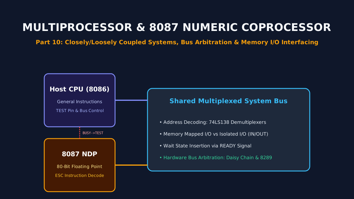
Part 10: Multiprocessor Configurations, 8087 Numeric Coprocessor, and Memory/IO Interfacing
Architectural principles of multiprocessor systems: closely vs loosely coupled topologies, hardware bus arbitration, the Intel 8087 floating-point NDP, and memory-mapped vs isolated I/O interfacing.
By Md. Harun-Or-Roshid
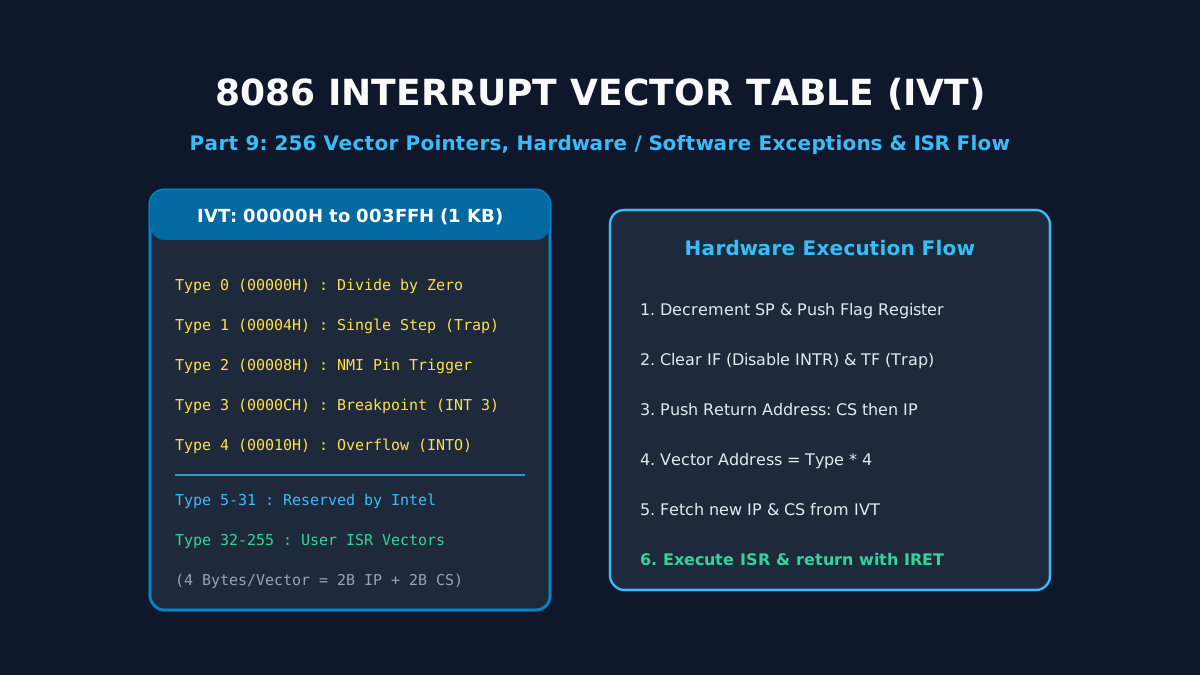
Part 9: Interrupt Structures and Vector Pointer Table in Intel 8086: Hardware, Software, and Exception Handling
A deep dive into 8086 interrupt processing: the 1 KB Interrupt Vector Table (IVT), dedicated Type 0–4 exceptions, hardware NMI/INTR lines, the 6-step interrupt response cycle, and the IRET sequence.
By Md. Harun-Or-Roshid
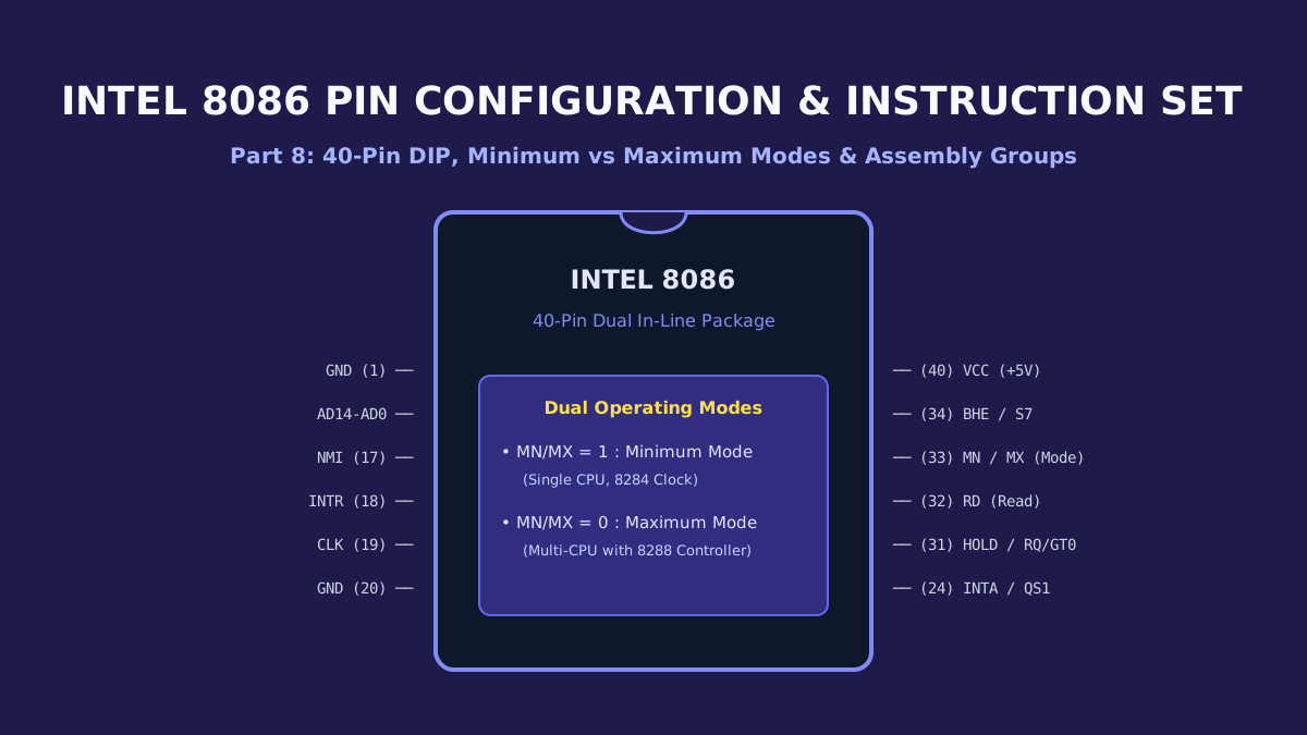
Part 8: Intel 8086 Pin Configuration, Operating Modes (Min/Max), and Comprehensive Instruction Set
Exhaustive hardware guide to the 40-pin Intel 8086: multiplexed address/data pins, Minimum Mode uniprocessor vs Maximum Mode multiprocessor circuits with the 8288 bus controller, and complete instruction set categorization.
By Md. Harun-Or-Roshid