Part 3: Intel 8085 Microprocessor Architecture: Internal Hardware, Registers, and Bus Demultiplexing
The Benchmark of 8-Bit Computing
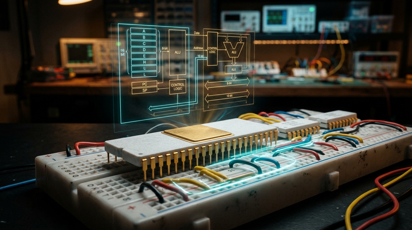
Introduced by Intel in 1976, the Intel 8085 is an 8-bit NMOS microprocessor that established the standard pedagogical blueprint for computer engineering. Operating from a single +5V DC power supply at a typical clock frequency of 3.072 MHz, the 8085 integrates an 8-bit ALU, an extensive register array, an internal clock generator, a multiplexed address/data bus, and five levels of hardware interrupts into a 40-pin Dual In-Line Package (DIP). In Part 3, we dissect its internal silicon layout, flag status logic, and the essential engineering circuitry required to demultiplex its low-order bus.
1. Functional Units of the Intel 8085
Internally, the 8085 architecture is partitioned into five distinct functional blocks communicating over an internal 8-bit bidirectional data bus:
1. Arithmetic and Logic Unit (ALU) & Accumulator
The 8-bit ALU performs arithmetic calculations (addition, subtraction, increment, decrement) and logical operations (AND, OR, XOR, complement, rotate). One of the inputs to the ALU is always provided by the Accumulator (Register A), an 8-bit register that also serves as the default destination for arithmetic/logical results. The second operand enters via a non-programmable Temporary Register.
2. The 8085 Status Flag Register
The 8085 contains an 8-bit register consisting of 5 flip-flops that record condition codes reflecting the outcome of the most recent ALU operation. Three bits are unused and held undefined.
- Sign Flag (S - Bit 7): Set to 1 if the most significant bit (D7) of the result is 1, denoting a negative binary number in two's complement notation. Cleared to 0 otherwise.
- Zero Flag (Z - Bit 6): Set to 1 if the ALU result is exactly zero ($00\text{H}$). Cleared to 0 if the result is non-zero. Crucial for loop counter termination (e.g.,
JNZ). - Auxiliary Carry Flag (AC - Bit 4): Set to 1 if a carry is generated out of bit D3 into bit D4 during arithmetic addition. Used exclusively by the
DAA(Decimal Adjust Accumulator) instruction for BCD arithmetic. - Parity Flag (P - Bit 2): Set to 1 if the result contains an even number of 1-bits (even parity). Cleared to 0 if the number of 1-bits is odd.
- Carry Flag (CY - Bit 0): Set to 1 if an arithmetic addition generates a carry out of bit D7, or if a subtraction requires a borrow into D7. Also manipulated by rotate and carry-control instructions (
STC,CMC).
3. General Purpose & Special Purpose Register Array
| Register | Width | Pairing | Function & Role |
|---|---|---|---|
| B, C, D, E, H, L | 8-bit each | BC, DE, HL | General-purpose data registers. May be used individually as 8-bit registers or paired as 16-bit register pairs. The HL pair serves as the default 16-bit memory pointer ($M$). |
| Program Counter (PC) | 16-bit | None | Holds the memory address of the next sequential instruction byte to be fetched. Increments automatically during opcode fetch cycles. |
| Stack Pointer (SP) | 16-bit | None | Points to the top of the stack structure in external Read/Write RAM. Decremented by 2 before a PUSH or CALL; incremented by 2 after a POP or RET. |
| W, Z (Temporary) | 8-bit each | WZ | Internal scratchpad registers used exclusively by the CPU control unit to hold temporary 16-bit addresses during XCHG, CALL, and LDA. Not accessible to programmers. |
2. Timing and Control Unit Signals
The Timing and Control Unit generates the clock pulses and control strobes that synchronize internal operations and external bus transactions. Key signal pins include:
- Clock Signals: $X_1$ and $X_2$ are input pins connected to an external quartz crystal (e.g., 6.144 MHz). An internal divide-by-2 flip-flop generates the operational system clock frequency (3.072 MHz) outputted on
CLK OUT. - Control Signals: $\overline{\text{RD}}$ (Read, active LOW indicates read transaction), $\overline{\text{WR}}$ (Write, active LOW indicates write transaction).
- Status Signals: $\text{IO}/\overline{\text{M}}$ distinguishes between Input/Output operations (HIGH) and Memory operations (LOW). Paired with $S_1$ and $S_0$ to identify current machine cycle:
Machine Cycle IO/M# S1 S0 Active Control Strobe Opcode Fetch 0 1 1 RD# = 0 Memory Read 0 1 0 RD# = 0 Memory Write 0 0 1 WR# = 0 I/O Read 1 1 0 RD# = 0 I/O Write 1 0 1 WR# = 0 Interrupt Acknowledge 1 1 1 INTA# = 0 Halt Z 0 0 None
3. Demultiplexing the 8085 Address/Data Bus ($AD_0 - AD_7$)
To minimize the physical pin count and fit within a standard 40-pin DIP footprint, Intel multiplexed the lower 8 bits of the address bus with the 8-bit data bus onto pins 12 to 19, labeled $AD_0$ through $AD_7$.
During the initial clock cycle of any machine cycle (clock state $T_1$), these pins output the lower 8 bits of the memory address ($A_0 - A_7$). During subsequent clock states ($T_2, T_3$), the same physical pins transition to transmit bidirectional data ($D_0 - D_7$).
The Demultiplexing Circuit (74LS373 Octal Latch)
To provide external memory with a stable, static 16-bit address for the entire duration of the read or write cycle, an external transparent octal D-latch (such as the 74LS373) is deployed:
- The CPU's $AD_0 - AD_7$ pins connect directly to the data inputs ($D_0 - D_7$) of the 74LS373 latch.
- The CPU asserts its Address Latch Enable (ALE) pin HIGH during clock state $T_1$.
- The HIGH pulse on ALE enables the 74LS373 latch, causing the lower address bits ($A_0 - A_7$) to pass through to its outputs.
- As the clock transitions to $T_2$, ALE drops LOW, latching and holding $A_0 - A_7$ steady on the output pins of the 74LS373 until the next $T_1$ state.
- The 8085 is now free to use pins $AD_0 - AD_7$ for bidirectional data transfer while external RAM reads the stabilized address lines $A_0 - A_{15}$ (where $A_8 - A_{15}$ originate directly from the unmultiplexed upper address pins 21–28).
Summary & Next Step
In Part 4, we build upon this physical foundation by analyzing the 8085 instruction encoding formats (1-byte, 2-byte, and 3-byte instructions), the five addressing modes, and the machine cycle timing diagrams that govern opcode fetch and memory execution.
Related reading
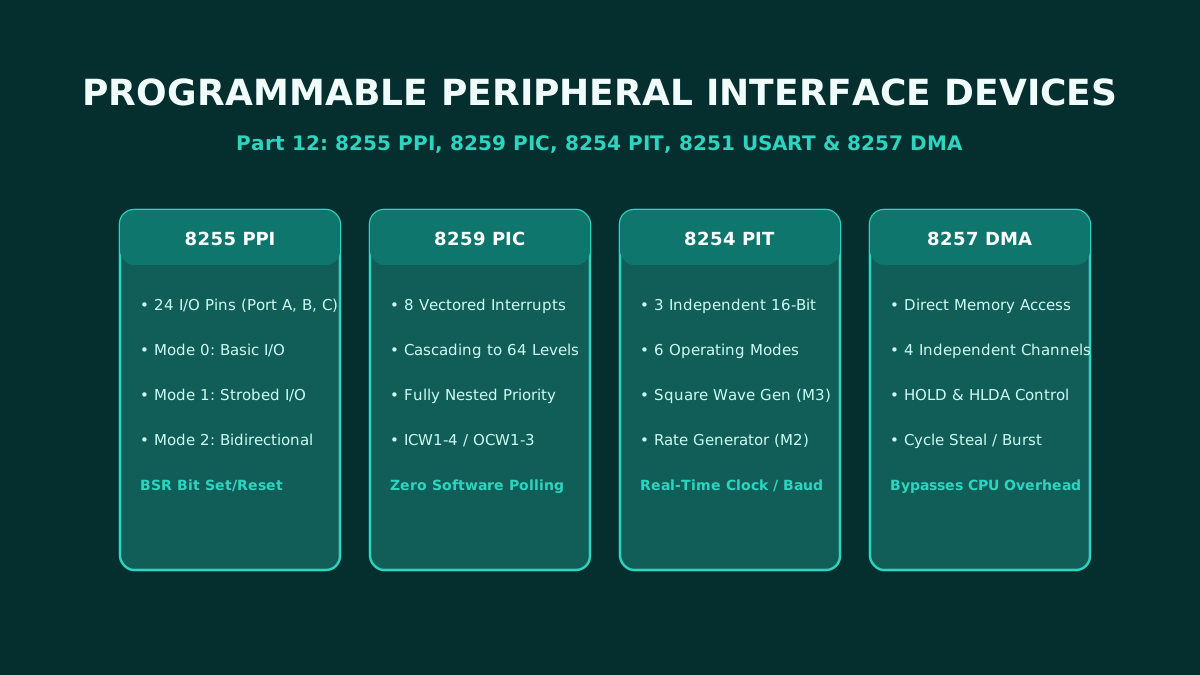
Part 12: Programmable Peripheral Interface ICs: Architecture and Pin Configuration of 8255, 8259, 8254, 8251, and 8257
The ultimate hardware reference for microprocessor peripheral interface adapters: complete architecture, pin configurations, and control word programming for the 8255 PPI, 8259 PIC, 8254 PIT, 8251 USART, and 8257 DMA controller.
By Md. Harun-Or-Roshid
Part 11: Intel 8051 Microcontroller Architecture: Harvard Memory Map, SFRs, and I/O Port Circuits
A master-level architectural analysis of the Intel 8051 microcontroller: Microprocessor vs Microcontroller paradigm, Harvard memory organization, 128-byte internal RAM layout, SFR registers, and internal circuits of Ports 0–3.
By Md. Harun-Or-Roshid
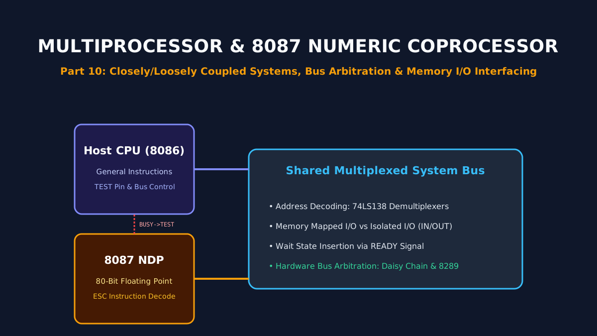
Part 10: Multiprocessor Configurations, 8087 Numeric Coprocessor, and Memory/IO Interfacing
Architectural principles of multiprocessor systems: closely vs loosely coupled topologies, hardware bus arbitration, the Intel 8087 floating-point NDP, and memory-mapped vs isolated I/O interfacing.
By Md. Harun-Or-Roshid
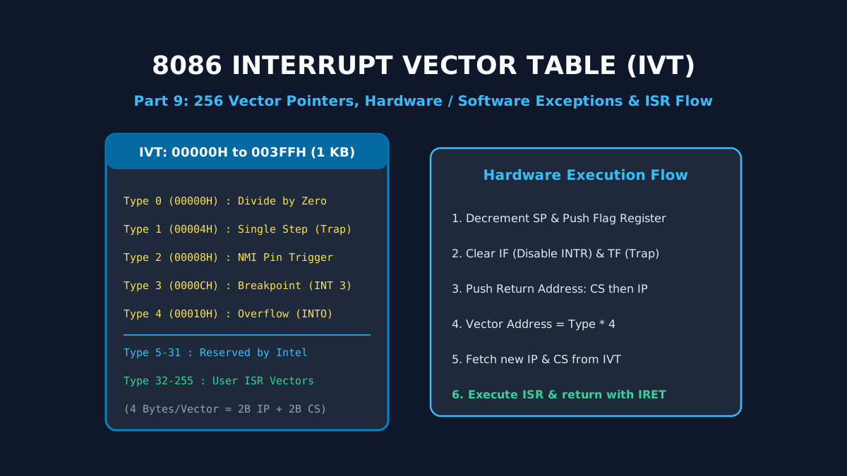
Part 9: Interrupt Structures and Vector Pointer Table in Intel 8086: Hardware, Software, and Exception Handling
A deep dive into 8086 interrupt processing: the 1 KB Interrupt Vector Table (IVT), dedicated Type 0–4 exceptions, hardware NMI/INTR lines, the 6-step interrupt response cycle, and the IRET sequence.
By Md. Harun-Or-Roshid