Part 1: Microprocessor Evolution, Architectural Generations, and Operating Fundamentals
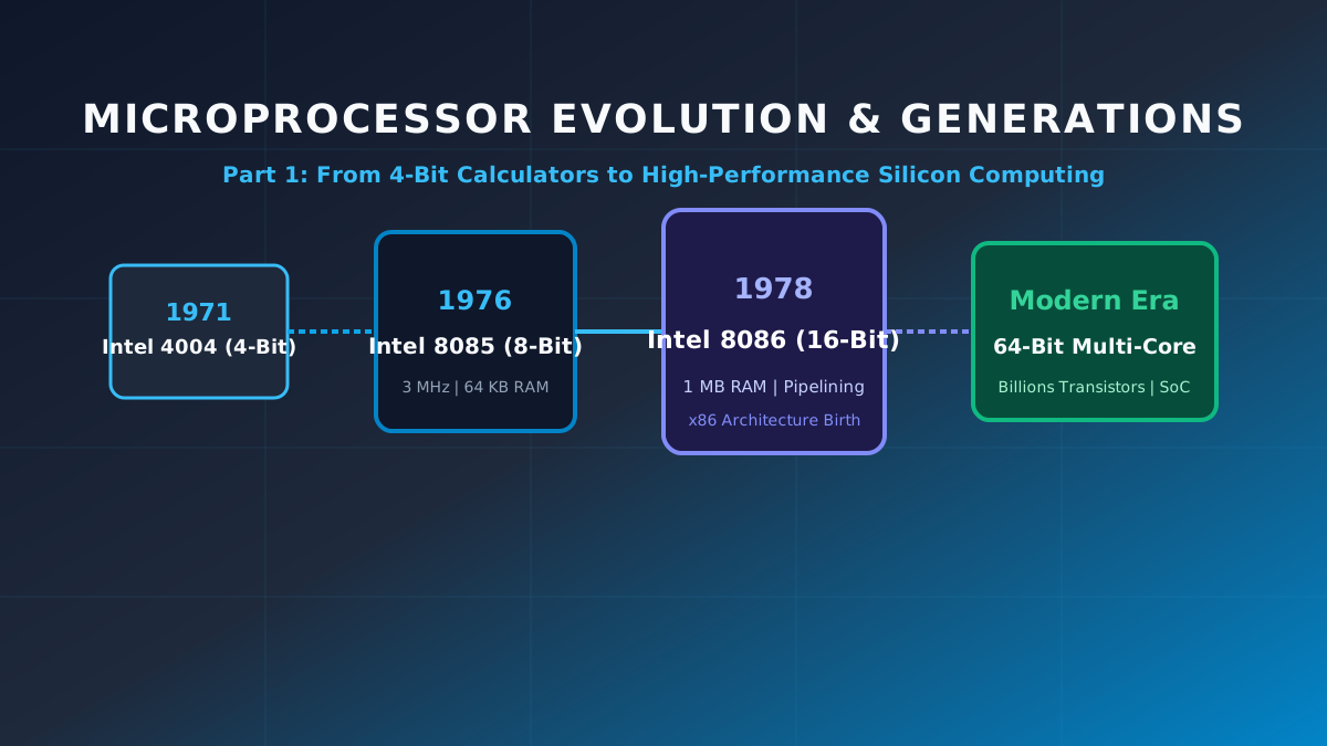
Series Overview & Learning Objectives
The invention of the microprocessor revolutionized modern civilization, condensing the entire Central Processing Unit (CPU) of a computer onto a single microchip of silicon. In this opening installment of our 12-part comprehensive engineering series, we examine the fundamental architecture of microprocessors, dissect the five architectural generations spanning from 1971 to the present, define critical performance metrics (MIPS, CPI, bus throughput), and trace the physical machine cycle that governs all digital computation.
1. What is a Microprocessor?
A microprocessor is a programmable, clock-driven, register-based electronic semiconductor device fabricated on a single Integrated Circuit (IC) using Very Large Scale Integration (VLSI) or Ultra Large Scale Integration (ULSI) technology. It serves as the primary computational engine and decision-making brain of digital computing systems.
Unlike dedicated hardware logic circuits (such as hardwired state machines), a microprocessor is inherently multipurpose. It operates by fetching binary instructions from an external or internal memory subsystem, decoding those instructions through internal control logic, fetching necessary data operands, executing arithmetic or logical manipulations, and producing output results or storing data back into memory. Any computing system engineered around a microprocessor as its primary central processor is formally categorized as a microcomputer.
Clock-Driven
Synchronized by periodic crystal oscillator pulses. Each micro-operation occurs on discrete clock state transitions (T-states).
Register-Based
Contains high-speed, on-chip temporary storage locations (Accumulator, General Purpose, Program Counter, Stack Pointer) for zero-latency operand access.
Programmable
Executes user-defined instruction sequences stored in memory without requiring physical rewiring of the underlying silicon circuitry.
2. Five Architectural Generations of Microprocessors
Microprocessor evolution is structured across five distinct architectural eras, characterized by exponential increases in transistor count (governed by Moore's Law), wider data word lengths, higher operating frequencies, and shifting semiconductor fabrication technologies (from PMOS to NMOS, CMOS, and FinFET/GAA).
| Generation | Era | Word Width | Semiconductor Tech | Representative Processors | Key Architectural Breakthroughs |
|---|---|---|---|---|---|
| 1st Gen | 1971–1973 | 4-bit / 8-bit | PMOS (High voltage, slow) | Intel 4004, 4040, 8008 | First single-chip commercial CPU; 2,300 transistors; 740 kHz clock; designed initially for Busicom desktop calculators. |
| 2nd Gen | 1974–1978 | 8-bit | NMOS (Faster, TTL compatible) | Intel 8080, 8085; Zilog Z80; Motorola 6800 | Single +5V power rail (8085); internal clock generation; vectored hardware interrupt pins; 64 KB address space; widespread adoption in industrial controllers and early personal computers (Altair 8800). |
| 3rd Gen | 1978–1981 | 16-bit | HMOS (High-density NMOS) | Intel 8086, 8088; Z8000; Motorola 68000 | Birth of x86; 1 MB physical memory addressing via segmented registers; instruction prefetch queue (pipelining); hardware multiply/divide instructions; minimum/maximum operating modes. |
| 4th Gen | 1981–1992 | 32-bit | HCMOS | Intel 80386, 80486; Motorola 68020/68030 | 32-bit flat memory addressing (4 GB); hardware memory management unit (MMU) supporting paging and protected mode; on-chip L1 cache and integrated numeric math coprocessor (80486DX). |
| 5th Gen & Modern | 1993–Present | 64-bit | Sub-micron CMOS, FinFET, GAA | Intel Core/Xeon, AMD Ryzen, ARM Cortex-A, Apple M-Series | Superscalar execution (multiple instructions per clock); branch prediction; out-of-order execution; multi-core CMP; heterogeneous big.LITTLE topologies; integrated neural processing units (NPUs). |
3. Critical Architectural Terminology & Metrics
Word Length / Word Size
The number of binary bits that the processor's internal Arithmetic Logic Unit (ALU) can process in a single operational cycle. An 8-bit processor (such as the 8085) operates primarily on 8-bit data words; a 16-bit processor (such as the 8086) manipulates 16-bit words natively. Larger word lengths correlate directly with arithmetic precision, register width, and internal data processing throughput.
Address Bus vs. Data Bus
Microprocessors interact with external memory and peripheral hardware through parallel conductors known collectively as system buses:
- Address Bus (Unidirectional): Carries the physical memory address from CPU to memory/peripherals. A bus of width $n$ bits can directly address $2^n$ unique memory locations. For example, 8085 has a 16-bit address bus ($2^{16} = 65,536\text{ bytes} = 64\text{ KB}$), whereas 8086 has a 20-bit address bus ($2^{20} = 1,048,576\text{ bytes} = 1\text{ MB}$).
- Data Bus (Bidirectional): Transfers raw data and instruction opcodes between the CPU, memory, and I/O devices. The width of the external data bus defines the quantity of information transferred per read or write bus cycle.
- Control Bus (Composite): Individual signal lines carrying synchronization, direction, and timing strobes (such as Read $\overline{\text{RD}}$, Write $\overline{\text{WR}}$, and Input/Output over Memory $\text{IO}/\overline{\text{M}}$).
Clock Speed, CPI, and MIPS Calculation
Processor throughput cannot be evaluated by clock frequency alone. It is governed by the classic iron law of processor performance:
Where CPI denotes Cycles Per Instruction, and MIPS (Million Instructions Per Second) measures raw instruction execution rate:
4. The Fundamental Machine Cycle (Fetch-Decode-Execute)
Every instruction executed by a microprocessor undergoes a deterministic hardware sequence called the Instruction Cycle, composed of one or more Machine Cycles (such as Opcode Fetch, Memory Read, Memory Write), which are themselves partitioned into discrete crystal clock cycles known as T-states.
Instruction Fetch (IF)
The CPU places the content of the Program Counter (PC) onto the address bus. The memory subsystem reads the location and returns the 8-bit instruction opcode across the data bus into the CPU's internal Instruction Register (IR). The PC automatically increments to point to the next contiguous byte.
Instruction Decode (ID)
The internal Instruction Decoder translates the bit-pattern within the Instruction Register. Control logic generates microcode pulses that configure multiplexers, register enables, and ALU data paths for that specific operation.
Operand Fetch (OF) / Memory Access
If the decoded instruction requires external data operands (such as an immediate constant or memory location), additional memory read cycles are initiated to load the operands into temporary working registers.
Execution (EX) & Writeback (WB)
The ALU performs the specified arithmetic (addition, subtraction) or logical operation (AND, OR, XOR), updates status condition flags (Zero, Carry, Sign), and commits the result to the destination register or writes it back to external RAM.
Summary & Next Step
In Part 2, we investigate the fundamental taxonomic classifications of microprocessors: CISC versus RISC architectures, EPIC computing, Vector and SIMD Array processing units, and superscalar execution pipelines.
Related reading
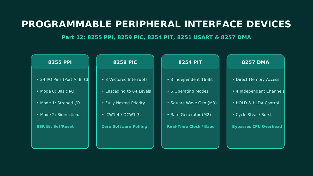
Part 12: Programmable Peripheral Interface ICs: Architecture and Pin Configuration of 8255, 8259, 8254, 8251, and 8257
The ultimate hardware reference for microprocessor peripheral interface adapters: complete architecture, pin configurations, and control word programming for the 8255 PPI, 8259 PIC, 8254 PIT, 8251 USART, and 8257 DMA controller.
By Md. Harun-Or-Roshid
Part 11: Intel 8051 Microcontroller Architecture: Harvard Memory Map, SFRs, and I/O Port Circuits
A master-level architectural analysis of the Intel 8051 microcontroller: Microprocessor vs Microcontroller paradigm, Harvard memory organization, 128-byte internal RAM layout, SFR registers, and internal circuits of Ports 0–3.
By Md. Harun-Or-Roshid
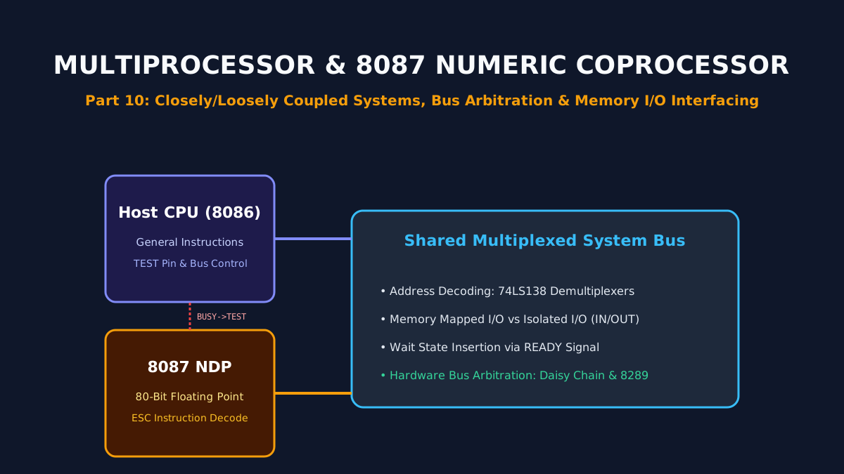
Part 10: Multiprocessor Configurations, 8087 Numeric Coprocessor, and Memory/IO Interfacing
Architectural principles of multiprocessor systems: closely vs loosely coupled topologies, hardware bus arbitration, the Intel 8087 floating-point NDP, and memory-mapped vs isolated I/O interfacing.
By Md. Harun-Or-Roshid
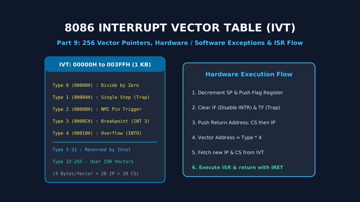
Part 9: Interrupt Structures and Vector Pointer Table in Intel 8086: Hardware, Software, and Exception Handling
A deep dive into 8086 interrupt processing: the 1 KB Interrupt Vector Table (IVT), dedicated Type 0–4 exceptions, hardware NMI/INTR lines, the 6-step interrupt response cycle, and the IRET sequence.
By Md. Harun-Or-Roshid